f2022-public-labs
Lab 5: Pulse-Width Modulation
Checkoff Demonstration Point Breakdown
| Step | Associated Steps (and checkoff criteria) | Points |
|---|---|---|
| 1 | 2. PWM (PC6-PC9 flashing in expected pattern, test PSC=480, check brightness) | 25 |
| 2 | 3. PWM Output Configuration (RGB ramps up to full white and back to off) | 25 |
| 3 | 4. PWM Sine Wave Synthesis (sine wave on PA11 on scope/AD2, adjustable with “A 440 #”) | 25 |
| 4 | 5. setrgb (change RGB color and intensity using “D RR GG BB”) | 25 |
| 7. Submit your code to Brightspace before the end of your lab section. | * | |
| Total | 100 |
* Your points are contingent on the submission of your code to Brightspace.
1. Introduction
A microcontroller’s interaction with the real world (and real humans) often requires the generation of voltages that can vary over a continuous spectrum. Although your microcontroller has an on-board digital-to-analog converter (DAC), it is too weak to drive any load that requires high power. Even with amplification, a DAC is inefficient for the purpose of driving heavy loads. Digital electronic systems are well-suited to switching circuits on and off. In circumstances where a load can be switched on and off in such a way that the average output voltage is treated (or perceived) as the signal, a solution is Pulse-Width Modulation (PWM). In this experiment, you will learn about configuring and using PWM to control a high-power load (a light) and generate a variable duty-cycle waveform.
1.1 Instructional Objectives (100pts total)
- To set up a basic concept demonstration of pulse-width modulation. (25 points)
- Implement a more complicated demonstration of pulse-width modulation. (25 points)
- To synthesize a waveform using PWM. (25 points)
- To control the color of an RGB LED using PWM. (25 points)
1.2 Wiring for this lab
For this lab, you will use a USB oscilloscope (such as a Digilent Analog Discovery 2 or an Analog Devices ADALM2000) to observe the timer PWM outputs.
Figure below shows the wiring for the new components for this lab. Be sure to leave all of the other lab 7 wiring in place. You will be using it for number entry and display. The LOW-PASS signal can be connected to the audio jack (where the DAC was connected to from the previous lab). A set of powered speakers will have a high impedance and can be directly connected to the LOW-PASS signal. If you’re using it to drive low-impedance headphones or earbuds, you should use the LM324 op-amp between the LOW-PASS signal and the headphones.
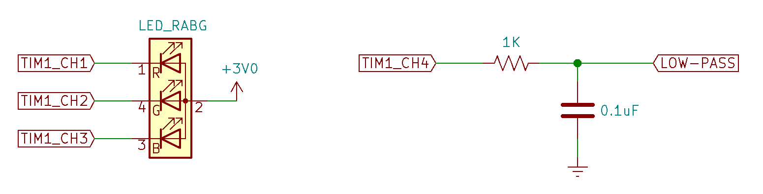
The RGB LED looks like a white LED with four leads rather than two. The RGB LEDs in your lab kit are common-anode devices. The anode is connected to 3 V, and each of three color component LEDs has a separate cathode. By connecting a cathode to a low voltage, the particular color of the LED is illuminated. In an additive color scheme red, green, and blue combine to produce white light. Remember that, since the cathodes of the LEDs are connected to the pins of the STM32, they will be illuminated when the pin outputs are in the low state.
Note: RGB LED datasheet
Under most circumstances, we would want to include limiting resistors in series with the LEDs. In this case, we want the LED output to be as bright as possible because we will dim each color by varying the PWM ON time of each channel. Each color of the RGB LED is able to tolerate the maximum current per pin that can be sunk by the STM32.
Note: You’ll have to look these up in the datasheet under the alternate function pinouts section…
TIM1_CH1TIM1_CH2TIM1_CH3TIM1_CH4
2 Pulse-Width Modulation (PWM) (25 Points)
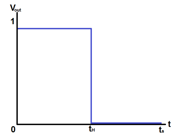
Consider a digital logic circuit which outputs a repeating, periodic signal over a known time period, $t_{S}$. Within the signal period, the circuit can output logic ‘1’ for a subinterval, $t_{H}$, and for the remaining time, outputs a logic ‘0’. This is illustrated in the figure below:
Expanding on the output above, suppose the circuit can be made to vary the logic ‘1’ interval $t_{H}$ to any value between 0 and $t_{S}$. A variety of potential outputs could result:
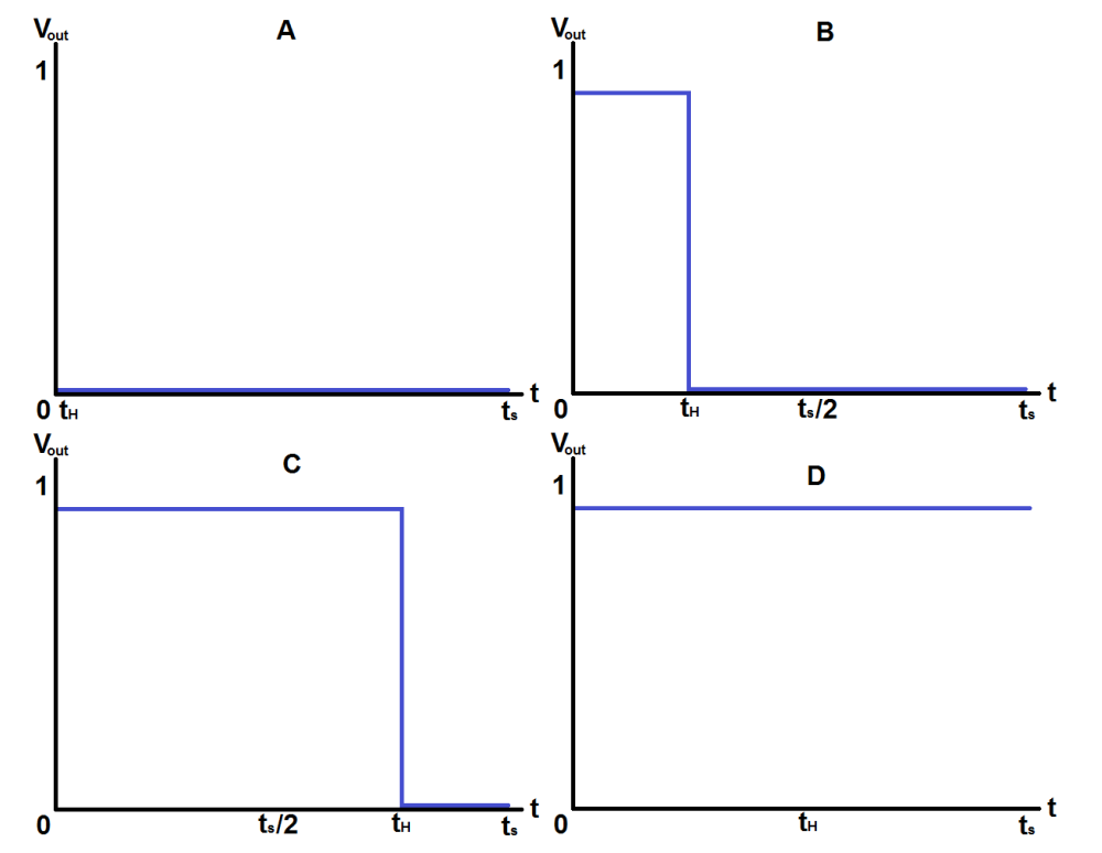
The relationship between the time the periodic signal spends high ($t_H$) and the total period of the repeating signal ($t_S$) is known as the signal’s duty cycle and is usually expressed as a percentage. In the figure above, signal A could be said to have a 0% duty cycle, signal B, 25%, C, 75%, and D, 100%. By controlling the duty cycle of the repeating, periodic output signal, a pulse-width modulator is capable of controlling average delivered current or power to a given load, and can further be used, possibly in conjunction with filtering, for crude approximations of analog values. Sometimes these values must be low-pass filtered to yield an analog value. For devices such as LEDs, the human visual system acts as a natural low-pass filter.
2.1 PWM on the STM32F0
On STM32 microcontrollers, pulse-width modulation is integrated into the various TIM peripherals. For the purposes of this experiment, TIM1 and TIM3 will be used for PWM outputs; you may wish to revisit the basics of timer operation from Lab 7.
As with all other peripheral configurations, the first step for configuring a peripheral is to enable the clock signal to it. This is done within the reset and clock control (RCC) system of the processor. Use of PWM, as well as other non-analog microcontroller peripherals, requires the use of alternative pin input functions. Alternate pin functions are detailed in the pin definitions table of the STM32F091RCT6 datasheet. Alternate function mode is specified using the GPIOx_MODER register for the appropriate GPIO port. Some pins can have more than one alternate function associated with them; specifying which alternate function is to be used is the purpose of the GPIOx_AFRL and GPIOx_AFRH registers.
Each timer peripheral that supports PWM on the STM32F0 features 4 independent channels, each of which can be set up to output a PWM signal. Specifying a channel as a PWM output requires writing to the TIMx_CCMRx registers. In PWM mode, the PWM frequency is specified through the TIMx_ARR register and duty cycles of the channels are controlled through the TIMx_CCRx registers. Aside from specifying alternate function mode on the associated I/O, additional steps must be taken in order to route the PWM signal from the internal peripheral to the external I/O pin. PWM is part of the timer’s capture/compare subsystem, thus the capture compare output for the selected channels must be activated in the timer capture/compare enable register, TIMx_CCER. The TIM1 subsystem is very similar to the TIM3 subsystem which was studied at length in lecture. One difference with TIM1 is that it has a “break and dead-time register” (BDTR). We will not use these features for this experiment, but the MOE bit of this register must be enabled to generate output on any of the channels of TIM1. At the end of timer configurations, remember to enable the timer, in the TIMx_CR1 register. For further assistance in setting up PWM, consult the example in Appendix A.9.8 of the family reference manual.
You will use three PWM channels to control an RGB LED, a device where the human visual model already acts as a low-pass filter. You will use a fourth PWM channel as an analog synthesizer output similar to that of the DAC in lab experiment 4. In this lab experiment, you will configure timer 1 for autonomous PWM operation. Other timers will invoke interrupts that read from the keypad, update the 7-segment display, and update the PWM duty cycle.
2.2 Preliminary Experiments with Timer 3
Complete the setup_tim3 subroutine to visualize what PWM channels look like. The code should do the following:
- Enable GPIO C port in RCC
- Configure
PC6 - PC9to be the outputs of Timer 3 channels 1 - 4. These are the four LEDs on your development board. - We give them to you here to save time. You’ll have to figure out the PA pins later. These route to the LEDs on the board.
- Enable the RCC clock for Timer 3.
- Configure Timer 3 prescaler to divide by
48000. - Configure Timer 3 for PWM mode 1 so that each channel output can have a CCR value between 0 and 1000:
- Configure the
ARRso that the timer update rate is 1 Hz. - Set each of the
OCxMfields of theTIM3_CCMR1andTIM3_CCMR2registers to set up PWM mode 1 (110). - Enable the four channel outputs in the
TIM3_CCERregister. - Enable the Timer 3 counter.
- Configure the
- Set each the Timer 3 CCRx registers as follows:
TIM3_CCR1= 400TIM3_CCR2= 400TIM3_CCR3= 200TIM3_CCR4= 100
Once these steps are done, uncomment the #define TEST_TIMER3 stanza in main().
Have a TA check you off for this step. (TA Instructions: You should see the lights for PC6 - PC9 flashing in the expected pattern. Ask the student to change the Timer 3 prescaler to 480 instead of 48000. You should see that the LEDs now have an apparent brightness proportional to their CCR value).
3 PWM Output Configuration (25 Points)
no new background here. We’re just making a more well-engineered PWM setup using stuff from earlier in the course.
The functions for the rest of the setup rely on functions from previous labs. You can either:
- Figure out and implement the functions yourself (this gives you the necessary practice for a possible lab practical), or;
- Use the solution object provided below (okay for the short term and getting checked off, but you might feel like putting off implementing them, which does NOT prepare you for the lab practical).
Read below only if you did not finish lab 4. Skip to “End solution section” if you already finished lab 4.
The functions provided in the solution object are:
void soln_setup_dma(void)
void soln_enable_dma(void)
void soln_setup_adc(void)
void soln_init_tim6(void)
void soln_TIM2_IRQHandler()
void soln_TIM7_IRQHandler()
void soln_init_tim15()
void soln_init_tim7()
void soln_init_tim2()
Here’s the solution object file that you’ll import into Eclipse, similar to how you used the autotest functions. Download this file and place it in the “src” folder of your project folder. To import this file into Eclipse:
- Right click on the project in Project Explorer.
- Click Properties, and you should see this window:
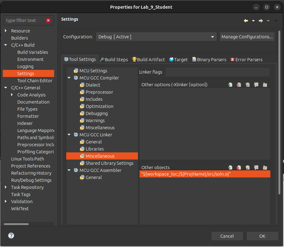
- Click through C/C++ Build > Settings > Tool Settings > Miscellaneous and use the Add object button (the one with a tiny green plus) under “Other Objects” to add the dma_adc_dac_soln.o file to the list.
Once imported, simply substitute any calls to the missing functions with the corresponding solution function, using the function names above. For the IRQHandlers, remember that the name cannot be different, so you’ll need to call the solution function inside the current IRQHandler instead.
End solution section
Copy the functions you completed for lab experiment 4 into the main.c file for lab experiment 5. For the demonstrations below, you should be able to use the keypad to enter information to demonstrate the things you implement.
Copy the implementation of following subroutines from your lab 4 main.c to your lab 5 main.c:
enable_ports(),setup_dma(),enable_dma(),init_tim15(),init_tim7(),setup_adc(),init_tim2(),init_wavetable(),set_freq(),init_tim6(), and- the ISRs for each of the timers
Implement the C subroutine named setup_tim1() that configures Timer 1 for PWM operation and routes the output to the external pins used for TIM1_CH1, TIM1_CH2, TIM1_CH3, and TIM1_CH4. (These are distinct from TIM1_CH1N, TIM1_CH2N, etc, which are the negated version of the same functions.) By now, you should know how to look up which physical pins can be used for these “functions”. Looking those up will also inform you how to set the alternate function configurations. Your subroutine should do the following:
WARNING: IF you accidentally overwrite the GPIOA AFRH (usually, using an
=sign instead of an|=or&=) you will turn off the programming port, which resides in port A. You will start getting “device not found” or “wrong device detected” messages. To rectify this mistake, you need to hold the reset button and run (not debug) your program.
- Activate the RCC clock to GPIO Port A.
- Configure the
MODERfor the four pins to set them for alternate function use. - Set the alternate function register to route the timer function to the external pins. The alternate function register is actually an array of two registers (
GPIOA->AFR[0]andGPIOA->AFR[1]). You will have to choose the correct array element to update. - Activate the RCC clock to Timer 1.
- You will be using Timer 1 for PWM output rather than interrupt generation. In order for output to work at all you must enable the
MOEbit of the break and dead-time register (BDTR). Do that now so you don’t forget. - Set the prescaler to divide by 1, and set the
ARRso that an update event occurs 20000 times per second. - Configure the output channels of Timer 1:
- Configure the “capture/compare mode registers”,
CCMR1andCCMR2, to set channels 1, 2, 3, and 4 for PWM mode 1. There are two 3-bit fields in each register that must be adjusted to accomplish this. - Configure the
CCMR2register to set the “output compare preload enable” bit only for channel 4 (OC4PEbit). - Enable the (uninverted) channel outputs for all four channels by turning on the CC1E, CC2E, etc. bits for in the “capture/compare enable register”,
CCER. Until you do this for each channel, the timer will not affect the outputs. - Enable the timer.
- Configure the “capture/compare mode registers”,
This configuration is long and tedious, and it won’t work at all if you set slightly wrong bit patterns (Your instructor has done this dozens of times and still has to ask “What did I forget?”). When it does not work, remember that you are in good company. Patience and diligence is strongly encouraged.
You will know when you succeed in getting the timer and channels configured properly, because the LED will be illuminated bright white. Spend a little time setting values in the CCR1, CCR2, and CCR3 registers. Use the I/O Registers control panel in SystemWorkbench to update them interactively. You might want to use use an oscilloscope to see the effect of setting a value in the register on the duty cycle of the PWM output. Initialize the CCRx values their maximum value, 0xffff, to ensure that the PWM outputs remain high, and the LEDs remain off. This will ensure you are not blinded in the time it takes to write the control software to change the intensity of the LEDs.
Finally, note that is is entirely possible to use the update event of Timer 1 to raise the interrupt that recomputes analog samples. That’s maybe too much complexity for this lab. It’s easier to set it up standalone and reuse the code from lab 4 to produce the waveforms.
Once these steps are done, comment the #define TEST_TIMER3 stanza in main() and uncomment the #define TEST_TIM1 to demo your work for timer 1.
Have a TA check you off for this step. (TA Instructions: Student’s LED should continually ramp up from dim to bright white. Check the setup_tim1() function too).
4 PWM Sine Wave Synthesis (25 points)
4.1 Synthesizing a Waveform with PWM
With low-pass filtering of the PWM output, the PWM duty cycle forms an analog output. The duty cycle is determined by the TIMn_CCRx value divided by the TIMn_ARR+1. As long as at least one full PWM cycle passes for every change in duty cycle, it will work as well as a DAC. A higher PWM frequency means a shorter period, which means fewer cycles in which to vary the duty cycle. This means there is a trade-off between the PWM frequency and the PWM duty cycle resolution.
NOTE: If you’re in 301 or have completed 301, you’ll probably see why we can do this. If you haven’t made it that far yet, you’ll be there soon enough. High frequency patterns make low frequency signals. Low pass filters remove the high frequency patterns, so you have the low frequency output leftover.
In lab experiment 4, we updated the DAC output 20000 times per second with 12-bit resolution (0 – 4095). If we wanted to update the PWM duty cycle 20000 times per second, with the highest resolution, we would take the following steps:
- Set the prescaler to divide by 1 (Set
TIMn_PSCto 0). Remember that is permissible to set the PSC to zero. Never set the ARR to zero though. - Set the ARR so that the counter updates (goes back to zero) 20000 times per second. For a 48 MHz clock, that means the counter should have a cycle of 2400 clock ticks between update events.
- The highest meaningful
CCRxvalue is then theARR+1, so there are 2401 distinct PWM duty cycle settings.
A range of 0 – 2400 is a little more than half the resolution of the DAC. If we used a PWM frequency of 10 kHz, it would allow a CCRx range of 0 – 4800, but 10 kHz is in the audible range, so the noise would make the resulting signal sound rather bad for higher tones.
4.2 Implementation
For this experiment, you will use a PWM frequency of 20000 for the sole reason of being able to do analog synthesis at the same rate you did in lab 4. The PWM frequency is, arguably, too high for LEDs. LEDs have a response time and the on-off rate is better at around 100 Hz, but the effect is not terribly degraded at 200 times this rate. It is certainly high enough that your eyes will not perceive any flickering.
Using a PWM update rate of 20 kHz means that you can take the wavetable synthesis subroutines from lab 4, and use them with only two changes:
- Instead of writing to
DAC_DHR12R1, you will write toTIM1_CCR4. There is no need to “trigger” the “conversion”. - Since the range of the duty cycle is 0 – 2400, rather than a range of 0 – 4095 for the DAC, the final sample should be shifted right by 18 rather than 17. A value of 1200 should be added center the duty cycle at 50% rather than adding 2048, which was the center value for the 12-bit DAC output.
Other than these changes to the Timer 6 ISR, all other subroutines like init_wavetable(), set_freq(), and setup_timer6() are the same as before.
Make the following changes outlined in the background section:
- Turn off
TRGOgeneration for Timer 6 (comment out theTIM6->CR2line in yourinit_tim6()). - Reduce the final combined sample with (in your TIM6 ISR):
sample = ((sample * volume)>>18) + 1200;
- Instead of writing sample to the DAC
DHR12R1register, write it to Timer 1CCR4.
WARNING: A common thing that’s forgotten about is that we have that potentiometer on the board. Remember these from lab 4? They adjust the amplitude of your output waveform. If you’re getting a signal that’s sitting at around 1.5V, your potentiometer is probably turned down to zero, and you need to turn it up.
Note: You may see an interesting problem if you do the
sampleupdate in one statement. Thevolumedefinition we gave you is auint32_t. That means that it is a 32-bit unsigned integer. The expression(sample * volume)is a signed type times an unsigned type, which is promoted to an unsigned type. When the offset is in the negative part of the wavetable, that product should be interpreted as negative. Hmm. When shifting a negative number as a signed type right, the most significant bit (a one) is duplicated. When shifting an unsigned type right, the most significant bit is always made zero. That means that a negative value is being turned into a very large positive value. When you add 1200 to it, it gets even larger. This math worked fine when we were assigning it to the 12-bitDHR12R1register in lab 4. Now, the CCR4 register is a 16-bit register. Those upper 4 bits are not chopped off. This will manifest itself as a value written to CCR4 that is much larger than 2400. So the value will be clipped at 100% duty cycle for about half the the sine wave. When you see this behavior, there are three ways to fix it. Choose one:
- Change the
uint32_t volume = 2400;line and replace “uint32_t” with “int” to make it a signed type.- Split the
sample = ((sample * volume)>>18) + 1200;into multiple statements so that a signed value is shifted rather than the unsigned product.ANDthe final computed (sample * volume) with0xfffto limit it to a 12-bit positive value. That way it will work withCCR4as well as it did withDHR12R1.
NOTE: A common problem we see that students choose to do all of these statements, which breaks their code. To reiterate, you only need to pick one of the above three statements. They provide the same output.
Once these steps are done, comment the #define TEST_TIM1 stanza in main() and uncomment the #define MIX_TONES to demo your work for this step. You can use the keypad as previous lab to set the frequency. To view the waveform, connect the oscilloscope probe to the LOW-PASS signal.
Notice that the more slowly-changing waves in the center appear to be thicker than the waves that quickly range from 0 to 3 V. This thickness is due to the 20 kHz PWM noise that is always either pushing the capacitor higher or pulling it lower. Figure below shows more detail of the synthesized waveform:
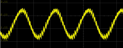
The center of the jagged wave represents the desired signal and the jagged edges represents the noise signal. The size of the deviation from the desired signal is significant. If this were an application where such deviations would affect the operation of a piece of equipment, filtering could be used to further diminish the 20 kHz content of the waves. For instance, if you could substitute a 10 KΩ resistor for the 1 KΩ resistor, you will see a much smoother waveform even at high magnification.
If the end result is to produce an audible waveform, the 20 kHz noise content will not be audible to human ears. Dogs and cats will be greatly bothered by it. It may also cause greater power dissipation in an amplification system.
Have a TA check you off for this step. (TA Instructions: Student should demonstrate a sine wave output on PA11 using the oscilloscope or AD2 that is adjustable from the keypad by pressing A 440 # (440 Hz sine wave))
5 setrgb() (25 points)
Several subroutines are provided for you that will read entire floating point and RGB number sets from the keypad while giving feedback on the seven-segment displays. The value returned by the getrgb() is a 6-digit BCD (4-bit representation of decimal digits) value to represent the RGB value to display using the RGB LED in the format 0xrrggbb. For instance, 0x009900 would be the maximum possible value for green (99) and the red and blue components turned off (00). The value 0x010005 would be the smallest visible illumination of red (01) and a slightly higher amount of blue (05). The example code in main() passes the return value of getrgb() into setrgb().
Write the C subroutine named setrgb() so it picks apart its argument (which is a value constructed by getrgb()) and uses it to set the TIM1_CCR1, TIM1_CCR2, and TIM1_CCR3 registers to set the red, green, and blue illumination appropriately. For instance, if the value is 0x112599, the duty cycle for the output connected to the red LED should be set so that it illuminates the red LED 11% of the time. The green LED should be illuminated 25% of the time, and the blue LED should be illuminated 99% of the time. (Using this scheme, it will not possible to set the PWM output to illuminate any of the colors 100% of the time.)
You cannot treat the number passed to setrgb() as a normal decimal integer. For instance, the BCD value 0x112599 is 1123737 if you look at as a two’s-complement binary integer. How will you turn that into the RGB components for the LED? It’s important that you think of it as six separate 4-bit BCD integers. To extract the numbers, remember that you can shift (») and mask (&) the value to look at different parts. For instance, if you entered the RGB value 0x123456, you can find the ten’s-place of the red component by shifting the value right by 20 and looking at only the four least significant bits by ANDing it with 0xf. To get the one’s-place of the red component, you would shift the value right by 16 and AND it with 0xf.
Note: A helper function
uint8_t bcd2dec(uint8_t bcd)has been provided to convert a byte in BCD form to decimal.
Remember that the LEDs are on when the corresponding PWM output is low, so a little more calculation will be necessary to make the LEDs have the proper intensity.
Once these steps are done, comment the #define MIX_TONES stanza in main() and uncomment the #define TEST_SETRGB to demo your work for this step.
The user interface code in main() works as follows:
- Press D followed by a 6-digit RGB value to set the three color components of the LED.
- Press A or B followed by the digits on the keypad to specify the frequency to use for the two sine waves. The ‘*’ button is the decimal point. Press ‘#’ to accept the number.
For instance, to produce a sine wave with a frequency of 426.386 Hz, press:
A 4 2 6 * 3 8 6 #
All of the analog waveform synthesis is generated using PWM channel 4 of Timer 1.
Button ‘D’ allows you to input a six-digit BCD RGB value to control Timer 1 PWM channels 1, 2, and 3. For instance, to set red to 1%, green to 9%, and blue to 5%, you would press:
D 0 1 0 9 0 5
Just enter the 6-digit BCD number. No terminating ‘#’ is needed.
Have a TA check you off for this step. (TA Instructions: Student should demonstrate changing the RGB LEDs color/intensity using the keypad.)
6. On Your Own
In semesters past, this lab has been constructed to also allow adjustment of the PWM frequency as well as the duty cycle for LEDs. That would have complicated the calculations needed to do waveform synthesis. You might try, on your own, the steps needed to control the frequency. Use the getfloat() subroutine for entry, and use the number to form the nearest possible PSC divisor. When doing so, it is still possible to use the waveform synthesis subroutines, but it will be necessary to change the RATE #define to a global floating-point variable.