f2022-public-labs
Lab 4: DMA, DAC, and ADC
Checkoff Demonstration Point Breakdown
| Step | Associated Steps (and checkoff criteria) | Points |
|---|---|---|
| 1 | 3. Wiring and enable_ports (check function implementation) |
5 |
| 2 | 4. DMA Transfer to 7-Segment Displays (uncomment SCROLL_DISPLAY) |
20 |
| 3 | 5. Debouncing Keypad (uncomment SHOW_KEY_EVENTS) |
15 |
| 4 | 6. ADC (uncomment SHOW_VOLTAGE) |
30 |
| 5 | 7. DAC (uncomment ONE_TONE, then MIX_TONES, test dialer()) |
30 |
| Total | 100 |
NOTE: Do not forget to do step 8 - you may want that code in the future.
NOTE: Do not forget to submit your code to Brightspace before the end of your lab section.
1. Introduction
In this lab, you’ll learn to use three peripherals: DMA, DAC, and ADC. All three of these are critical components in most chips in some way, shape, or form.
Direct Memory Access (DMA) allows you to automatically transfer a region of memory to a peripheral, a different location in memory, or any memory mapped region of the device. In short, it sets up automatic memory transfers from one thing to another. These can be peripherals, variables, arrays, etc. Just not flash ROM. You may ask, how is this useful? Well, instead of taking up valuable CPU time and additional code structures to transfer data, you can just have one of the DMA coprocessors do it. They’re independent and autonomous, so once you set them up, they just go. You’ll see more interesting applications in lab 10 and 11. Here, you’ll use it to collect ADC data.
Interfacing a microcontroller with real-world devices often means working with analog voltages that are not constrained by digital logic’s high/low dichotomy. In this lab, you will gain experience using the digital-to-analog converter and the analog-to-digital converter built in to your microcontroller. You will also practice writing code to manipulate the converted values as well as display them on an output device.
2. Instructional Objectives
- To understand the concept of analog-to-digital conversion
- To understand the concept of digital-to-analog conversion
- To learn how to use STM32F0 peripherals to measure and process analog information
- To use DMA to automatically transfer data to and from peripherals
3. Experiment Setup (5 points total)
Download the template project folder from lab website.
For this lab experiment, you are provided many support subroutines that do interesting and useful things with the peripherals that you configure. In the past, we’ve asked students to write some of them on their own – with mixed results. These subroutines are sometimes difficult to fully test without using them. Often, students’ work passed our tests without actually functioning correctly.
Fundamentally, this course is not a programming class, per se. For this lab, you will write only the code to configure and enable the peripherals you use. You can look at the support code to see what it does and how it does it. The file is support.c.
3.1 Wiring for this lab
Note: Don’t kill your board. Be very careful about what pins you may accidentally bring in contact, and pay attention to the notes that follow.
For this lab we will keep the wiring from lab 7 and add some other circuitry related to ADC and DAC. In addition, you will use an oscilloscope to observe the output of the DAC. If you haven’t learned how to use an oscilloscope yet, you can use an AD2 or read the guide on how to use the lab equipment in the Brightspace (as of 3/13 has not been posted, but will sometime soon).
You will use potentiometers to connected between 3V and GND with the center tap acting as a voltage divider. The center tap of the potentiometer will be connected to an analog input. As long as you are certain to connect the potentiometers only between 3V and GND, no damage to the analog inputs is possible.
Note: The output capacitor on the buffer can be either 10 or 100uF. I just don’t have a great way to get that across in a schematic.
NOTE: DO NOT give anything else aside from the output buffer 5V power. You will kill your development board. The transistors inside the LM324 will saturate and give incorrect output signals if you give it only 3V, which is why in needs 5V.
NOTE: DO NOT assume that the LM324 has the same pins for power and ground as your 74-series chip - they are not pins 7 and 14! Look up the datasheet for an LM324 to identify the power and ground pins.
3.2 enable_ports() (5 points)
Fill out the subroutine enable_ports() with the following configurations:
- Enables the RCC clock to
GPIOBandGPIOCwithout affecting any other RCC clock settings for other peripherals - Configures pins PB0 – PB10 to be outputs
- Configures pins PC4 – PC7 to be outputs
- Configures pins PC4 – PC7 to have output type open-drain (using the
OTYPERregisters) - Configures pins PC0 – PC3 to be inputs
- Configures pins PC0 – PC3 to be internally pulled high
As usual, you should not alter the configuration for any other pins. For instance, if you were to improperly alter the MODER setting for PC12, the serial port would stop working.
4. DMA Transfer to 7-Segment Displays (20 Points Total)
In lab 7, you set up a timer to periodically output 11-bit patterns on Port B GPIO pins to select a digit and present an 8-bit pattern on it. By doing so rapidly, you created the illusion that all eight digits were shown simultaneously.
In this lab you’ll do this again. Instead of using an ISR to set up the GPIO outputs, you will use the DMA subsystem to copy from an eight-entry memory buffer to copy 16 bits at a time into the ODR. That’s 5 more bits than you need, but they won’t matter as long as the upper 5 pins are not configured to be outputs.
4.1 Direct Memory Access
The STM32F09x family of microcontrollers have 2 Direct Memory Access (DMA) controllers, each with 7 and 5 channels respectively, that can autonomously move one or more words of various sizes between memory and peripherals. Once values are written to a DMA channel’s configuration registers, the CPU can be used for other purposes while the transfer operations continue. Each incremental DMA operation can be triggered by a peripheral’s readiness to be written to or read from. Some microcontrollers allow DMA channels to be arbitrarily associated with peripheral devices, but the STM32F0 requires that each peripheral be used with only the specific DMA channel that it is wired to. Table 32 and 33 of the Family Reference Manual shows the peripheral-to-DMA channel mapping. Find this table, as you’ll need it later.
A breakdown of how the DMA registers work:
CNDTR:A counter of sorts. You write the number of elements that you’re trying to transfer here. If it’s a singular variable, usually 1 is sufficient. If it’s an array, you must write in the size of the array. Stands for Channel’s Number of Data to Transfer Register.CMAR:The address of the memory location. This must be an address. You cannot insert just the variable/array. Stands for Channel’s Memory Address Register.CPAR:The address of the peripheral location. Again, this must be an address. Stands for Channel’s Peripheral Address Register.CSELR:This register lets you change how the initiated requests map out. Normally, each channel looks at a specific request. You can use this register to change what requests the channels looks at. We won’t use this one here, but we will use it later.
Then you have the control register, CCR. We suggest reading through the Family Reference manual thoroughly to find out how these work, but here’s some of the important ones:
MSIZE:A bit field that sets the size of the memory. Not all data is a full integer. You can select from quarter word, half word, and full word data sizes.PSIZE:Similar toMSIZE, not all peripherals have the same size of memory. Each GPIO has a 16-bit IDR, but the ADC might only take an 8-bit conversion. Set the size of your peripheral’s data with this field.MINC:A singular bit that shows if the memory address should increment. Typically, you use this if you’re using an array. The incrememnt size is also set by MSIZE.PINC:A singular bit that shows if the peripheral address should increment. Typically, this isn’t used unless you’re using this to copy from memory to memory.CIRC:A singular bit that tells the transfer to keep going. If this isn’t set, it’ll stop after it completes. If it’s set, it restarts each time it completes.DIR:A singular bit that sets the direction the transfer is taking. It can be memory to peripheral (writing a value to the ODR) or reading something into memory (writing a value from the IDR into a variable).
There are, of course, other things that you can do with this. For now, let’s stick with those definitions.
Last, each DMA channel can give updates on its progress by invoking interrupts. Three interrupts are possible:
- ‘TCI:’ The Transfer Complete Interrupt indicates that all datums of the DMA request have been moved.
- ‘HTI:’ The Half Transfer Interrupt indicates that half of the datums of the DMA request have been moved.
- ‘TEI:’ a Transfer Error interrupt indicates that an access was attempted to a memory location that was not permitted for the type of operation requested.
These are not required for this lab, or any others for that matter. However, they’re useful in practice as watchdog handlers, or for monitoring large data transfers. For example, playing a song with the micro requires a surprisingly large amount of data, and you need to refill the buffer consistently. Normally, you use a HTI flag to refill a buffer before it ends to make sure the song plays continuously.
4.2 Configure DMA transfers (10 points)
Here, you will set up a circular DMA transfer to the GPIOB peripheral’s ODR register to drive the seven-segment LEDs. The trigger will be triggered whenever TIM15 has an update event. As soon as the timer reaches the ARR value, the DMA channel will be triggered to write a new value into the data register.
Remember that TIM15 works with one particular channel of the DMA1 controller. You will find and use that default channel.
Remember that there are symbols that define the values you need to shift into registers, and you can find them by searching through the stm32f0xx.h file that defines all the symbols you use, eg. RCC and RCC_AHBENR_GPIOCEN. Use the symbols as a way of “being sure” that you are setting the right values in the right parts of the register.
Have you determined which DMA channel Timer 15 can trigger? Good. Implement the C subroutine named setup_dma() that does the following things:
- Enables the RCC clock to the DMA controller and configures the following channel parameters:
- Turn off the enable bit for the channel, like with every other peripheral.
- Set
CPARto the address of theGPIOB_ODRregister. - Set
CMARto the address of the msg array. - Set
CNDTRto 8. (the amount of LEDs.) - Set the
DIRection for copying from-memory-to-peripheral. - Set the
MINCto increment the CMAR for every transfer. (Each LED will have something different on it.) - Set the
Memory datumSIZEto 16-bit. - Set the
Peripheral datumSIZEto 16-bit. - Set the channel for
CIRCular operation.
Implement one more C subroutine named enable_dma() that does only the following operation:
- Enable the channel.
There is a lot of variation in students’ work. On occasions when we use autotest to check their work, it’s check all possible cases once a DMA channel is enabled and running. We want you get used to keeping this step separate. Remember to not enable the DMA channel in setup_dma.
4.4 init_tim15() (10 points)
Fill out the subroutine init_tim15() to enable TIM15’s clock in RCC and trigger a DMA request at a rate of 1 kHz. Do that by setting the UDE bit in the DIER, while not setting ‘UIE’. In this case, ‘UDE’ triggers DMA requests. ‘UIE’, which we’ve used in the past, causes interrupts. You may have noticed that we’ve not asked you to make an ISR for TIM15, because there is no ISR to invoke for this timer this time. The timer will trigger the DMA channel directly. Don’t forget to enable the timer as well.
This whole operation amounts to the DMA operation will do the copying that you had to do in the ISR in lab 5.
Once you implement these subroutines main(), you should see “ECE 362” on the 7-seg LED array. The interesting thing to notice here is that the circular DMA operation continually and automatically copies the buffer array msg to the display. This creates the illusion that the memory is mapped into the display.
Once you are ready for the actual demo, please comment out the for loop with asm("wfi") inside first. Otherwise the program won’t proceed any further.
4.4.1 When it doesn’t work…
So you’ve done all these steps and it does nothing. Is it time to call the course staff and have them just tell you exactly what to type?
(Just kidding. It’s never time to ask the course staff to tell you what to type.)
So many circumstances in this class depend on getting many details exactly correct before something works. Now, you have an opportunity to develop your debugging skills so that you are prepared for future situations. Here are the steps to take when using DMA. Invoke the program in the System Workbench debugger and use the I/O Register Debug panel to check registers one at a time to ensure they are correct. Here are the imporant ones:
- Is the program stuck in the DefaultHandler? Did something cause a fault?
- Is the RCC clock to Port B enabled?
- Are pins PB0 - PB10 configured as outputs?
- Look at timer 15:
- Is the timer enabled?
- Repeatedly click on the
CNTregister to update its view. Is it changing? If not, it probably means that the timer is not running. - Is the
CNTvalue larger than the ARR? That’s usually a sign that you set up the ARR after you set the CEN bit to enable the timer’s counter. Always set CEN last. - Did you set the
UDEtimer to trigger the DMA channel?
- Look at the DMA channel you’ve configured:
- Are you sure you picked the right DMA channel? Look at Table 32 on page 205 of the Family Reference Manual to check your assumption. Only one particular DMA channel will work with Timer 15. Make sure you use that one.
- Repeatedly click on the
CNDTRregister to update its view. Is it changing? If not, it probably means that the DMA channel is not being triggered or some configuration issue, explained below, is happening. - Did you set the
CMARandCPARaddresses properly? Look up the address of theGPIOB ODRin the I/O Register debugger. - Did you set the DMA channel direction to copy from memory to the
GPIOB ODR? - Did you set the
MINCbit to increment theCMARand clear thePINCbit to not increment theCPARafter each copy? - Did you configure the DMA channel for circular operation?
By systematically checking all of these elements, you can find the root cause(s) of any problem.
4.5 Demo time
Uncomment the #define SCROLL_DISPLAY stanza. This will define a symbol that will enable compilation of the code block enclosed in the #ifdef ... #endif below it.
Your LEDs should scrolling the Hello...Hello... string now.
4.6 How does it work?
Look at the code for print() in the support.c file. It copies one byte at a time into the msg[] array. For historical reasons, every ASCII character is defined by the lower seven bits of the byte. That let us use the most significant bit to indicate that the dot on a character should be set or not. This will be used in the code to show key events in the next section.
5. Bouncing, Debouncing, and Keypad Implementation (15 Points Total)
5.1: What is bouncing?
Buttons and switches are not perfect. Usually, there is some sort of spring to it, which means that the electricity “bounces” around inside of there. Unfortunately, it’s pretty good at wrecking data, and it’s hard to see with the untrained eye. When I press a switch, here’s an example of a zoomed out view:
When I zoom in really far, it looks something like this:
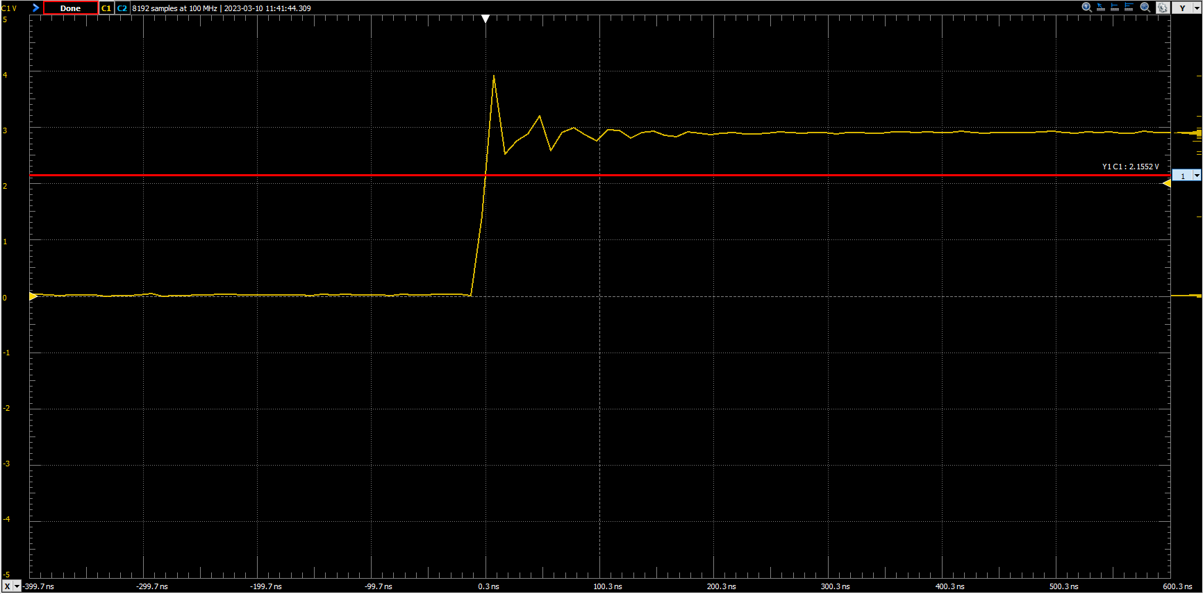
You’ll notice that I put in a red cursor that shows where the logic line is. This is a better bounce because it’s a nicer switch, and it doesn’t cross back over the logic line, so the input won’t oscillate. What happens when I use a switch that I found on my floor?
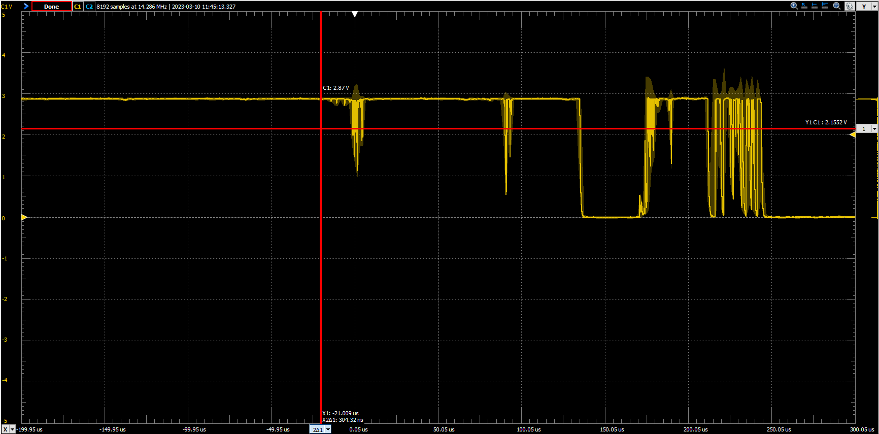
That looks like garbage, right? Notice that I have two red cursors on the screen that are separated by a singular pixel. Within this very slight time duration, the processor is able to look for an input around 15 times. The system doesn’t settle for another 250 microseconds, so it could be reading any of those oscillations! How do we fix this? Debouncing. We can do this in a hardware fashion or a software fashion. For the hardware fashion, we add a capacitor in parallel with the input like in lab 5.1. This creates a charge constant, and will smooth out high frequency noise. Here’s an example of when I add a 1uF capacitor in paralell with my input:
That looks a lot more decisive than the last picture. However, this isn’t the point of the lab, and I’m just including it so you can see exactly what this is in a hardware implementation, as we haven’t in the past.
Software debouncing is the point here, which is in this next section.
5.2 Software Debouncing a Keypad
In lab 7, you learned how to scan a keypad matrix. In this lab experiment, you will do that again. However, this time you will debounce the presses so that you can determine the moment each one is pressed and released, and do a translation of keys.
Briefly, a method called the history method keeps track of the last eight readings from each button on the keypad in a byte of memory. When the byte is 00000000, it has been idle for a long time. When the byte is 00000001, it has been read as pressed recently. When the byte is something like 10101011, it was pressed some time ago, and it is still bouncing. When the byte is 11111111, it has been pressed for a long time and is no longer bouncing. When the byte is 11111110, it has been read as recently released. In a sum, the history method waits to assign a keypress until the buttons has settled.
To detect multiple button presses, we would want to configure the keypad scanning outputs as open-drain (either pulled low or floating high) and enable pull-up resistors on the keypad scanning inputs. That way, each input would naturally float high, and any key press on a selected column would force a row low. This way different columns would not be high and low, and pressing two buttons in the same row no longer creates an indeterminate voltage level on the row. For instance, if Col1 was pulled low and the others were floating pressing the ‘4’ and ‘5’ buttons will only cause the Row2 output to go low. Col2 is not pulled high or low, so pressing the ‘5’ button does not interfere.
It would be simpler to understand if an output pin could be configured to either push high or float. This configuration is called open-source, and it is not supported by the STM32 GPIO system. (By the way, it has nothing to do with “open-source software”. The term has to do with the “source” pin on a MOSFET.) From an electrical standpoint, it is no better or worse to do so with open-drain outputs.
Each time a button is pressed or released, an entry will be placed in a circular queue. For the purposes of this lab experiment, a two-element queue will be enough. The main loop of your program will check the queue quickly and remove entries before it is filled up by a button press.
The subroutine to wait on keys and return their value will sleep waiting on interrupts and check the queue every time it wakes up. If there is something in the queue to indicate a button press, it will note what it is, translate it into the ASCII character representation, clear the queue entry, and advance to watching the next entry in the queue. By clearing each queue item after it is read, subsequent reads of the queue can recognize the presence of a new button press by looking for a non-empty queue entry.
Note: In this lab, you will be using pins on Port C for the keypad. This means you will modify the GPIOC_MODER configuration. Remember that, if you modify the configuration for pin PC12, you will disable the serial port. Double-check your MODER updates to make sure they will not change pin 12. We won’t use the serial port for this lab, but this kind of double check will be useful for future lab exercises when we use it again.
5.3 Timer 7 ISR (10 points)
Write the interrupt service routine for Timer 7. Be sure to copy its exact name from the startup/startup_stm32.s file so that you get the name correct. The code should do something similar to what you did in lab 7:
// Remember to acknowledge the interrupt here!
int rows = read_rows();
update_history(col, rows);
col = (col + 1) & 3;
drive_column(col);
First, the rows are read. Later, the column is updated. This allows for the R-C components that comprise any electrical circuit to charge up and stabilize in time for the next invocation of the ISR. If you look at the implementation of read_rows() and drive_column() in the support.c file, you will see that they are similar to the ones you used in lab 7, but they are inverted. Remember that we are using active-low signals with open-drain configuration to be able to read multiple button presses simultaneously.
In the middle of the code is a call to update_history() which keeps track of the past eight samples of each button. If any button’s history has the bit pattern 00000001, it means that the button has just now been recognized as pressed for the first time. If any button’s history has the bit pattern 11111110, it means that the button has just now been recognized as released for the first time. Either of these situations cause update_history to record the event in the two-entry queue[] array.
5.4 init_tim7() (5 points)
Implement the C subroutine named init_tim7() that causes the Timer 7 ISR to be invoked at a rate of 1 kHz. The steps that you use to accomplish this are similar to those that you underwent in lab 7.
5.4.1 When it doesn’t work
Use the System Workbench I/O Register Debugger to determine what the problem is when it does not work.
- Is the RCC clock enabled for Timer 7?
- Has the PC4-7 been configured with output type open-drain?
- Has the PC0-3 been configured with pull-high?
- Is the Timer 7 counter enabled?
- Repeatedly click on the Timer 7
CNTregister to update its value. Is it changing? If not, the timer is probably not enabled. - Is the
UIEbit set? - Has the interrupt source been enabled in
NVIC? - Set a breakpoint in the Timer 7 ISR. Is it ever invoked? If not, you may not have named it correctly.
5.5 Demo time
Put a comment before the previous #define SCROLL_DISPLAY stanza and then uncomment the #define SHOW_KEY_EVENTS. This will enable a call to the show_keys() subroutine, which does not return. It will continually call get_key_event() and display the result on the seven-segment display. Each time a key is pressed, get_key_event() returns the ASCII code for the key with the most significant bit set. On the seven-segment display, this is shown with the decimal point. When a key is released, get_key_event() returns the ASCII code for the key with the most significant bit clear.
If you press and hold the ‘1’ key, the display should show ‘1.’ (a ‘1’ with the decimal point lit). When you release it, a ‘1’ without the decimal point will be shown.
The interesting thing about using open-drain configuration to scan the keypad is that you can register a second button press without having to release the first one. Try pressing and holding the ‘1’ and ‘2’ keys. Release one at a time. See the results on the seven-segment display.
5.6 How does it work?
Look at the update_history() subroutine in support.c file. It uses the push_queue() subroutine to put new event entries in the two-entry msg[] queue. Then, look at the get_key_event() function. It checks the two-entry queue to wait for a non-zero value. It removes that value, using pop_queue and returns it. As an efficiency improvement, it embeds a WFI instruction so that it does not continually run. A button event can only happen as a result of an interrupt, so it doesn’t miss anything by waiting for the WFI to complete.
5.7 Why would I ever do this instead of hardware debouncing?
Mostly, cost. It’s cheaper to have an intern code this once into your software than to pay someone to assemble hundreds of extra resistors and capacitors.
6 Analog-to-Digital Conversion (30 Points Total)
Audio signals, analog sensor input waveforms, or input waveforms from certain types of input devices (sliders, rotary encoders, etc.) are all examples of analog signals which a microcontroller may need to process. In order to operate on these signals, a mechanism is needed to convert these analog signals into the digital domain; this process is known as analog-to-digital conversion.
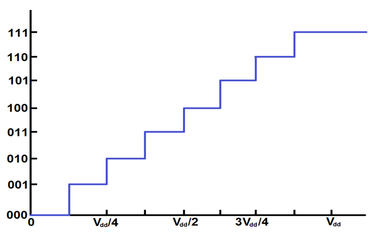
In analog-to-digital conversion, an analog signal is read by a circuit known as an analog-to-digital converter, or ADC. The ADC takes an analog signal as input and outputs a quantized digital signal which is directly proportional to the analog input. In an n-bit analog-to-digital converter, the voltage domain of the digital logic family is divided into 2n equal levels. A simple 3-bit (8-level) analog-to-digital quantization scheme is shown in the figure below:
There are several ways to lay out a topology scheme for an ADC. Below is an example of one that also happens to be a 3-bit decoder, although it is simplified a little:
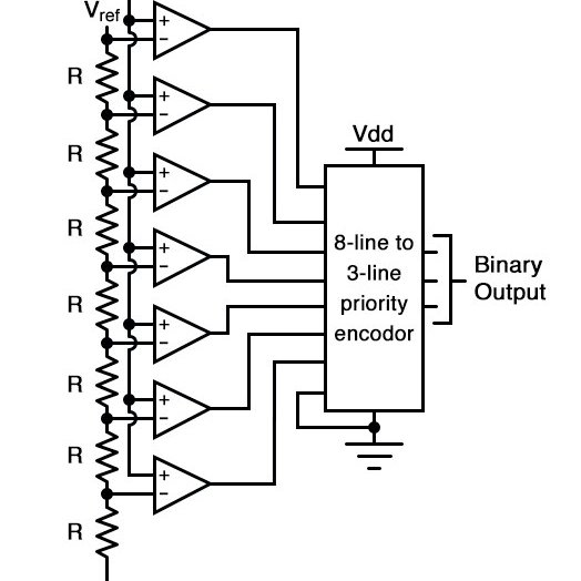
If this is something you’re interested in designing, you’ll need to do a little further reading elsewhere. Design of an ADC is an art, and we (unfortunately) do not have the time to cover it in this course.
In this section, you will set up the analog-to-digital converter (ADC) and repeatedly check it to update a global variable. Since there is always some amount of noise, you will smooth out the readings by creating a boxcar averaging mechanism and using that average to update a variable.
6.1 Configuring the STM32F0 ADC
The STM32F0 microcontroller has an integrated 12-bit analog-to-digital converter. The converter has 19 channels, allowing for readings from up to 16 independent external pins and three different internal sources. The ADC is capable of converting signals in the 0-3.6V range, although it is limited by the reference voltage on the development board (for ours, it’s approximately 2.95 V). It is able to capture and convert a new sample every 1μs. Many other ADC features are described in greater detail in the microcontroller documentation, and it’s worth a read when you have some free time. Namely, the ADC can look at 16 different inputs by multiplexing.
Before any ADC configuration can be done, a few initializations must be done. First, the ADCEN bit must be enabled using RCC, as was done with other peripherals in previous experiments. However, which bit in which register is that located? It is up to you to consult the documentation for the RCC registers to determine the right bit to set.
Next, the inputs which are to be configured as analog I/O must be configured for analog mode in the corresponding GPIOx_MODER register. This is described in further detail in section 9.3.2, “I/O pin alternate function multiplexer and mapping”, of the STM32F0 family reference manual.
Prior to performing any configuration of the ADC, the peripheral must first be enabled. ADC activation must take place before any other ADC configurations are performed; failure to follow this order may result in the ADC entering an unknown state, at which point the ADC must be disabled and restarted. This is backwards to how it’s normally done, which may not seem intuitive right away. That’s because it’s not.
Enabling the ADC requires writing ‘1’ to the ADC enable bit, ADEN, in the ADC control register, ADC_CR. Once this is done, software must wait until the ADC is in a ready state, indicated by the bit ADRDY (located in the ADC status register, ADC_ISR) being read as ‘1’ to software.
For the purposes of this experiment, we are interested in configuring the microcontroller ADC for single conversion, using the “software-driven mode.” This means that the ADC will perform a single conversion, initiated in software. The ADC will then await the next software trigger before another conversion is initiated. This is the default operating mode of the ADC, and no special configurations will be needed within the ADC peripheral. In the event that special operating conditions (DMA, continuous conversion mode, etc.) need to be performed by the ADC, operating modes can be specified via the ADC configuration registers: ADC_CFGR1 and ADC_CFGR2.
When performing a conversion, the ADC will read and convert values on any active channels. By default, all ADC channels are disabled. Prior to use, it is important to enable those channels on which conversions will be performed. This is done through the ADC channel selection register, ADC_CHSELR.
6.2 Using the STM32F0 ADC
Once the ADC has been properly enabled and configured, initiating an analog-to-digital conversion is as simple as writing a ‘1’ to the ADSTART bit in the ADC_CR register. Writing a ‘1’ to this bit instructs the converter to automatically begin conversion of all ADC channels. This bit will automatically be cleared by hardware once the conversion has completed. Converted ADC data is ready to be processed by the core once the end of conversion bit, EOC, is activated in the ADC_ISR register.
In some situations, particularly when disabling the ADC, it may be desirable to stop a conversion which is already in process. This can be done by writing a ‘1’ to bit ADSTP of the ADC_CR register. Doing so will stop the ongoing conversion process, discarding any data, and will automatically clear the ADSTART bit.
Once an analog-to-digital conversion has been completed, the converted data can be read from the ADC data register, ADC_DR. Data will be right-aligned or left-aligned, depending on configuration settings (right-aligned by default).
Note: It is worth reiterating that, when an external pin is configured for analog operation, it puts delicate internal circuitry at risk. If you expose an external pin to greater than 4.0 V even for a fraction of a second, it will permanently, irreparably damage either the pin or the entire microcontroller. Disconnect your microcontroller from power when you are wiring circuits. Don’t connect anything to the 5 V power pin of the microcontroller. Check your circuitry before applying power to your development board.
Note: In this lab, you will be using pins on Port A for analog operations. This means you will modify the
GPIOA_MODERconfiguration. Remember that, if you modify the configuration for pins PA13 or PA14, you will lose the ability to debug or even re-program the microcontroller. Double-check yourMODERupdates to make sure they will not change pins 13 or 14. Some of the newer TAs will not recognize this issue right away, and it will consume an hour of your time.When you misconfigure GPIO Port A, remember that you can restore the ability to use the debug/programming interface by:
- Repairing your program,
- Pressing and holding the reset (SW1) button,
- Pressing “Run” on SystemWorkbench to reprogram the microcontroller
Depending on what kind of mistake you made, you might have to hold down the reset button for only one second after pressing “Run”. You may also need to reprogram the microcontroller twice before it works again. Be patient. Do not give up. Ask a TA for help with this process.
6.3 setup_adc() (10 points)
Implement the C subroutine named setup_adc() that initializes the ADC peripheral and configures the pin associated with ADC_IN1 to be analog mode. To write this subroutine, you should carefully examine the example in the lecture on Analog-to-Digital Conversion. You should also consider examples A.7.2 and A.7.4 of the Family Reference Manual appendix. The subroutine should do the following:
- Enable the clock to GPIO Port A
- Set the configuration for analog operation only for the appropriate pin
- Enable the clock to the ADC peripheral
- Turn on the “high-speed internal” 14 MHz clock (HSI14)
- Wait for the 14 MHz clock to be ready
- Enable the ADC by setting the ADEN bit in the CR register
- Wait for the ADC to be ready
- Select the corresponding channel for
ADC_IN1in theCHSELR - Wait for the ADC to be ready
Your subroutine can use the default configuration of right-aligned 12-bit conversion. Really, not much more need be done than is shown in the example of the lecture. We just want to do the minimum needed to make the ADC work.
Hint: To find the pin associated with
ADC_IN1, Table 13 of the STM32F091x datasheet is a good starting point (page 34). Plus you can always search it in the document. Yet another Hint: Why enable GPIO port A for this section?
6.4 Timer 2 ISR (10 points)
Create the ISR for Timer 2. Set it up to do the following steps:
- Acknowledge the interrupt.
- Start the ADC by turning on the
ADSTARTbit in the CR. - Wait until the
EOCbit is set in the ISR. - Implement boxcar averaging using the following code:
bcsum -= boxcar[bcn];
bcsum += boxcar[bcn] = ADC1->DR;
bcn += 1;
if (bcn >= BCSIZE)
    bcn = 0;
volume = bcsum / BCSIZE;
This makes for a rather long-running ISR, but we actually want that to demonstrate the effects of interrupt priority in a later step.
6.5 init_tim2() (10 points)
Complete the init_tim2() subroutine so that it sets up Timer 2 to invoke the ISR exactly ten times per second (10 Hz).
6.5.1 When it doesn’t work
Use the System Workbench I/O Register Debugger to diagnose the problem:
- Is the RCC clock enabled for Timer 2?
- Is the Timer 2 counter enabled?
- Are the Timer 2
PSCandARRvalues as you expect them to be? - Repeatedly click on the Timer 2
CNTregister to update its value. Is it changing? If not, the timer is probably not enabled. - Is the
CNTvalue higher than theARRvalue? This is an especially important problem for Timer 2, where theARRandCNTregisters are 32 bits in size. It takes a long time to wrap around back to zero. You will have this problem if you enable the timer counter before you set theARR. - Is the
UIEbit set? - Set a breakpoint in the Timer 2 ISR. Is it ever invoked? If not, you may not have named it correctly, or you did not enable it in NVIC.
- Is the RCC clock for Port A enabled? Are the pins configured for analog operation? (Do you know which pin
ADC_INcorresponds to?) - Is the RCC clock for the ADC enabled?
- Look at the ADC ISR register. Is the ready bit set? Does the Timer 2 Interrupt Service Routine turn on the
ADSTARTbit? (The bits will change to quickly to read them in the I/O Register Debugger.)
6.6 Demo time!
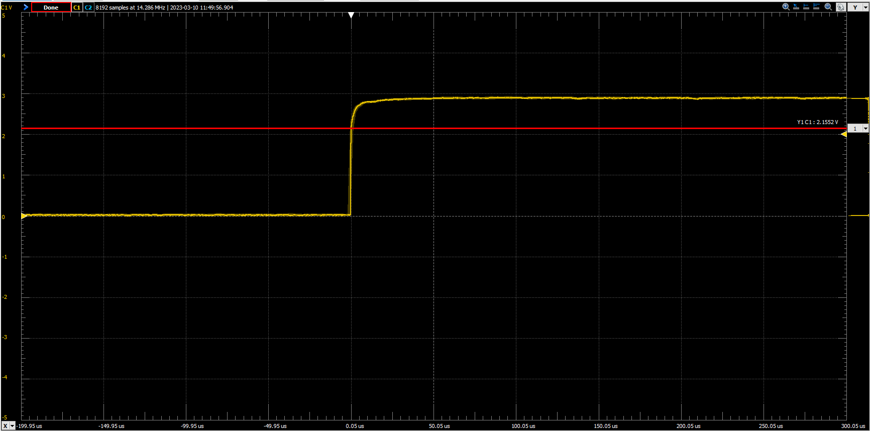
Re-comment the #define SHOW_KEY_EVENTS above and uncomment the #define SHOW_VOLTAGE stanza. This will enable code that continually calls printfloat() for a calculation that estimates the voltage on the ADC_IN pin.
Because the boxcar is 32 samples wide, and because new samples are only taken ten times per second, it will take about three seconds to converge on any new value. If you start the code with the potentiometer on full, it will gradually display values between zero and (approximately) 2.9. If you change the potentiometer, it will take another three seconds to converge on the new value. You can speed this up or slow it down by changing how quickly the timer refreshes. Remember, the ADC supports only up to 100kHz.
7 Digital-to-Analog Conversion (30 Points Total)
A digital-to-analog converter (DAC) is similar to analog-to-digital conversion in reverse. An n-bit digital quantity is written to a data register, the conversion is triggered, and the quantized analog value appears on an output pin. One significant difference is that, since the conversion mechanism uses only a resistor network, the conversion is nearly instant. There is no need to continually check a DAC to find out if the conversion is complete.
Like the ADC input, the DAC output cannot represent all values. For an n-bit DAC, there are 2n distinct values. A digital value of n zeros usually represents an analog conversion of 0 V. A digital value of all ones usually represents an analog conversion of the reference voltage: $$ V_{REF} $$ If treated as an n-bit integer, each increment results in an approximately: $$ V_{REF} / 2^n $$ volt increase in output voltage.
For the final step of this lab exercise, you’ll configure the DAC and an ISR to create and mix sine waves with arbitrary frequency.
7.1 Configuring the STM32F0 DAC
The STM32F091 microcontroller has an integrated 12-bit DAC with two output channels. Samples can be written to the DAC, converted, and alternately written to either channel to produce stereo audio. For this lab experiment, however, we will use only the first channel. (Read section 14.4 of the Family Reference Manual if you want to learn more about “Dual-Mode” output control.)
To configure and use the DAC, the RCC clock must first be enabled. The pin to use for analog output must be configured for analog mode by setting the appropriate value in its GPIOx_MODER register field. Next, DAC channel 1 must be enabled by setting the DAC_CR_EN1 bit in the DAC_CR register. Finally, the type of trigger to use to initiate a conversion must be selected. For this lab experiment, we’ll use a software trigger.
7.2 Using the STM32F0 DAC
Because it does not require polling to determine the completion of a conversion, use of the DAC is less complicated than the ADC. All that is necessary to produce an analog value on an DAC output when configured for software trigger mode, is to write a value into the appropriate Data Holding Register (DHR) and initiate the conversion by writing a ‘1’ to the trigger bit of the DAC_SWTRIGR register. The DAC is ready to receive another sample in the next APB clock cycle.
Like the ADC, the DAC has variable bit sizes as well as left-aligned and right-aligned data handling capabilities, but they do not need to be selected in advance. If you wish to output an 12-bit left-aligned data value, you write it to the DAC_DHR12L1 register before triggering the conversion. If it is a 12-bit right-aligned value write it to the DAC_DHR12R1 register instead. The only other bit size available is an 8-bit right-aligned register, DAC_DHR8R1. There is no left-aligned 8-bit data holding register, nor are there any other sizes.
It is important to understand that writing to any of the channel 1 holding registers (DAC_DHR12L1, DAC_DHR8R1, DAC_DHR12R1) effectively creates a holding register value equivalently. For example, doing any of the following three writes:
- Writing 0x0000d700 to DAC_DHR12L1 or…
- Writing 0x00000d70 to DAC_DHR12R1 or…
- Writing 0x000000d7 to DAC_DHR8R1
will deposit the 12-bit value 0xd70 into the 12-bit hardware register waiting to be converted by the DAC. They’re all equivalent cases. In normal operation, you just want to use the one that works best with your calculations.
7.3 Initialize a Wavetable
A subroutine named init_wavetable() that computes an N-entry sine wave and writes it into the array named wavetable[] is written for you to see. Each entry of the array is a signed 16-bit integer which can represent values from -32768 to 32767. For reasons of symmetry, your sine wave values should range from -32767 to 32767. This is done like so:
for(int i = 0; i < N; i++)
    wavetable[i] = 32767 * sin(2 * M_PI * i / N);
The STM32F091 has no floating-point hardware, so this will be computed with slow, emulated mechanisms. It is still fast enough that it can be done at program startup without being noticed. You must, however, avoid floating-point calculations in time-critical situations such as interrupt handlers.
7.4 set_freq()
A subroutine set_freq(int chan, float f) is provided for you. It updates one of two sets of global values that are the fixed-point step and offset into the wave table for the two channels.
7.5 setup_dac() (10 points)
Implement the C subroutine named setup_dac() that initializes the DAC peripheral and configures the output pin for DAC_OUT1 for analog operation. Consider the example on the lecture on Digital-to-Analog Conversion as well as the examples in Appendix A.8. Your subroutine should do the following:
- Enable the clock to GPIO Port A (reenabling is safe)
- Set the configuration for analog operation only for the appropriate pin
- Enable the RCC clock for the DAC
- Select a TIM6
TRGOtrigger for the DAC with theTSELfield of the CR register - Enable the trigger for the DAC
- Enable the DAC
You don’t need to disable the buffer-off (BOFF) bit or first disable the DAC enable before you set values. Just do the minimum necessary steps to enable the DAC as specified.
Hint: Again, to find the pin associated with
DAC_OUT1, Table 13 of the STM32F091x datasheet is a good start.
7.6 Timer 6 ISR (10 points)
Write the ISR for Timer 6. It should do the following to setup the next value to stage the next value for the DAC:
// Acknowledge the interrupt right here!
offset0 += step0;
offset1 += step1;
if (offset0 >= (N << 16))
    offset0 -= (N << 16);
if (offset1 >= (N << 16))
    offset1 -= (N << 16);
int samp = wavetable[offset0>>16] + wavetable[offset1>>16];
samp = samp * volume;
samp = samp >> 17;
samp += 2048;
DAC->DHR12R1 = samp;
The code accomplished the following things.
- Increment
offsetvariables by thestepamounts - If the integer portion of
offsetis greater than N, find the fixed-point representation of N and subtract it from the offset. (See the notes on sound generation.) - Get the sample from the
wavetableat index of the integer portion of offset. - Multiply the sample by
volume. - Shift the sample to the right by 17.
- Add 2048 to the sample.
- Write the sample to the 12-bit right-aligned data holding register of the DAC.
The sum of the two wavetable values will be between -65535 and +65535. The volume variable is a 12-bit number, so it has a maximum value of 4095. If this is multiplied by a sample the product will range between +/-268435456 (which is $\pm 2^{28}$). When this value is shifted right by 17, it will result in a signed 12-bit value. Adding 2047 to it will put it in the range 0 - 4095, which is appropriate for DAC output.
In order to realize a digital-to-analog conversion of a value written to the DAC data holding register (DHR12R1), it is necessary to trigger the DAC. In the lecture notes, you’ve seen this done by writing to the software trigger register, but the ISR shown above does not do this triggering. Instead, you configured the DAC to be triggered by the Timer 6 TRGO. Remember to set up Timer 6 to enable that.
7.7 init_tim6() (10 points)
A symbolic constant, RATE is defined in main.c. Implement the subroutine init_tim6() that initializes timer 6 so that it’s interrupt is called at RATE times per second (20000 for this exercise). It would be best if the code used RATE to calculate the values to use to set up the timer so that you can change RATE later.
Remember that timer 6 must be configured to trigger the DAC. To do so, look at the CR2 register for the “Master Mode Select” field. Set the value that enables a TRGO on an Update event.
7.7.1 When it doesn’t work
Use the System Workbench I/O Register Debugger to look at the values you’ve written to configuration registers. In particular:
- Look at the value in the DAC
DHR12R1register. Is it non-zero? Does it ever change? In a working system, you will see a change each time you update it. - If the
DHR12R1register does not change, set a breakpoint in the Timer 6 ISR. Is it ever invoked? Does it have the right name? Is the Timer configured correctly? - Step through the code in the ISR when it is invoked. Make sure it computes a new
DHR12R1value that is not always the same.
7.8 Demo time
Uncomment the #define ONE_TONE which reads a floating-point value from the keypad. To enter a decimal point, press *. To finalize the number entry, press #. For instance, to enter the value 466.164, press 4 6 6 * 1 6 4 # on the keypad.
The frequency should be produced on the DAC_OUT1 pin.
The potentiometer serves as a volume control for the output. If you connect earbuds or amplified speakers to the output, you should be able hear it clearly. You may also view the waveform produced on DAC_OUT1 with an Analog Discovery system.
You can also uncomment the #define MIX_TONES stanza to enable two-frequency mixing. Select a channel by first pressing A or B. Then enter the floating-point frequency as before. For instance, to produce a 261.626 Hz tone with channel 0 and a 329.628 Hz tone with channel 1, press the following keys:
A 2 6 1 * 6 2 6
B 3 2 9 * 6 2 8
Finally, if you comment all of the #define stanzas in the main.c file, it will fall all the way through to the invocation of the dialer() subroutine. This subroutine produces a North American dial tone. Pressing the buttons on the keypad produces the Dual-Tone Multi-Frequency (DTMF) tones that can be used to dial a phone. Pressing # re-dials the previously entered number (up to 16 digits). If you have a “land line” you can actually dial the phone by holding the handset microphone to a speaker connected to DAC_OUT1.
8 Interrupt Priorities
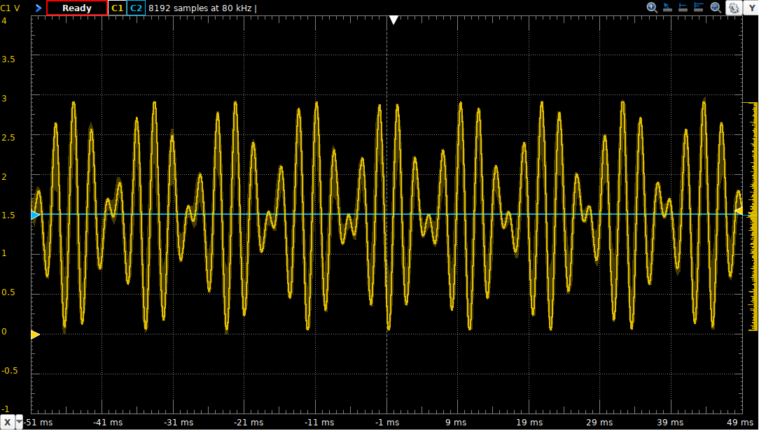
This is a good time to look at the effects of setting interrupt priorities and their effects on programs that have multiple interrupts. We chose to use Timer 2 for the ADC sampling specifically because it has a higher priority than the other timer interrupts. In other words, as long as the Timer 2 ISR is running, the Timer 6 ISR cannot be invoked. If the Timer 6 ISR is running when the Timer 2 interrupt is raised, the Timer 6 ISR will be preempted to allow the Timer 2 ISR to run.
Since Timer 6 is used to generate audio samples, it is very important that it have consistent timing. Any interference with its 20 kHz rate will be easily heard. To demonstrate this, add the following (useless) code to the Timer 2 ISR:
for(int x=0; x<10000; x++)
    ;
Then look at the output of a single sine wave generation on an oscilloscope (or simply listen to it). You will see a wave form that has interruptions that look like this:
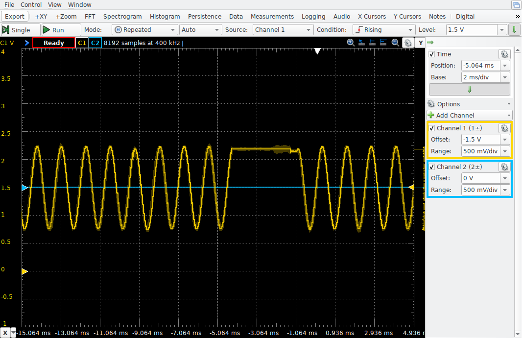
Since the Timer 2 ISR takes a long time to run, it prevents the Timer 6 ISR from putting new updates into the DAC DHR. To avoid problems like this, every ISR should be as short as possible. For instance, you didn’t notice this problem until the long loop was inserted into the Timer 2 ISR! Nevertheless, sometimes it is necessary to make long calculations in an ISR. Another solution would be to use a timer with a lower priority interrupt. That would ensure that the Timer 6 ISR ran on time. Another solution is to lower the priority of the Timer 2 interrupt. To do so, simply add the following line to the init_tim2 subroutine:
NVIC_SetPriority(TIM2_IRQn, 3);
Recall that the upper two bits of the ISPR register bytes define four allowed interrupt priorities, from highest-to-lowest: 0, 64, 128, and 192. For some unknown reason, the NVIC_SetPriority() subroutine is configured to simply specify only those two bits, so the values of the second argument are 0, 1, 2, and 3.