f2022-public-labs
Lab 3: Timers
- Lab 3: Timers
- 1. Introduction
- 2. Instructional Objectives
- 3. Background and wiring
- 3.1 Debouncing buttons (can be ignored since we won’t touch this until lab 8)
- 3.2 Reading a button matrix
- 3.3 Driving multiplexed displays
- 3.4 Use of a sink driver and high-side transistors
- 3.5 Tips for wiring the circuit
- (100 points) 4. Experiment
- 3. Playing the game
1. Introduction
Each timer subsystem allows the microcontroller to produce periodic interrupts while the CPU is busy with other operations. In this experiment, we will use timer interrupts to periodically scan a matrix keypad and reliably report button presses.
2. Instructional Objectives
- Learn how to configure the timer subsystem
- Use timer interrupts
- Scan a matrix of buttons
- Learn how to drive a multiplexed display
3. Background and wiring
3.1 Debouncing buttons (can be ignored since we won’t touch this until lab 8)
Because switches are mechanical devices, they bounce. This means we do not get a stable electrical signal on a press or a release. Because of switch bounce, the voltage fluctuates between VDD and ground before settling down to a stable value. There are several ways to fix this. Debouncing can be performed in hardware or software.
We used to make debouncing a central part of this lab experiment, however doing so in assembly language was a difficult exercise. We’ll do a better job in lab experiment 6. The following information is presented for your consideration on lab 6. For this lab, we won’t debounce the button presses. Instead, we’ll build an application that is tolerant of redundant detection of the same button.
1) Hardware debouncing: You have already seen this working well in previous labs (lab 3). Hardware debouncing is done via a simple RC network to filter high frequency glitches that occur from mechanical bounce. The Schmitt trigger inputs of the microcontroller can tolerate the relatively low speed of the signal changes.
2) Software debouncing: In certain applications it might be beneficial to debounce switches in software rather than use an RC filter on each switch.
Software debouncing can be achieved in a variety of methods. The simplest debouncing method is to read the voltage, wait for the switch to settle and read it again. However there are more robust approaches, which are more suited for a keypad matrix. Here we describe one such method that we call the “history method”.
In this “history” method we store N previous button states. Each button’s history is represented by a single variable. This variable is referred from here on, as the ‘history variable’. The least significant bit of the history variable represents the most recent button state and the most significant bit represents the oldest button state in history. When a new button state is read, the history variable is shifted left by one, making space for the new state in the least significant bit. The new state value (i.e. 0 or 1) is ORed into the history variable.
Now that we have a history of button states we can look for two specific patterns to identify a button press and release. An 8-bit pattern of 00000001 represents the first moment of a button press and 11111110 represents the first moment that of a button release. Note that these patterns are applicable when the button’s logic is active high, else the patterns are switched. Therefore, by checking if the history variable equals 1 (i.e. 00000001) we can detect a button press. Similarly by checking if history variable is 0xfe (i.e. 11111110) we can detect a button release.
3.2 Reading a button matrix
A matrix of buttons presents an additional complication to the challenge of debouncing since it is not possible to monitor each button separately. To understand why this is so, it’s helpful to discuss how a matrix keypad works.
You will use a 16-button keypad for this lab experiment. One configuration for such an arrangement of buttons would be to have two wires for each button (32 wires total) so that each button could be independently monitored. That would require a lot of pins on the keypad which might make it difficult to use on a breadboard. An optimization might be to have one common power connector and one more connector per button (17 wires total) so that each button could still be monitored individually. But this is still too many pins on the keypad than manufacturers will usually support, and the numbers would only be much worse for keypads with even more buttons.
The typical concession for keypads is to have multiple common pins that connect to groups of buttons. The logical extension to this trend is to configure a keypad as a matrix of rows and columns. If the number of rows and columns is about equal, this practice minimizes the number of pins on the keypad. The added challenge is that the keypad must be scanned one row or column at a time. For instance, a voltage can be applied to a column of buttons, and the rows can be sensed to detect if any of the buttons in the column are being pressed. Then the voltage can be removed from the column and re-applied to another column. By cycling through all the columns, all keys can eventually be detected. The difficulty is that, not only do the buttons still bounce, the bouncing must be tracked over multiple successive scans.
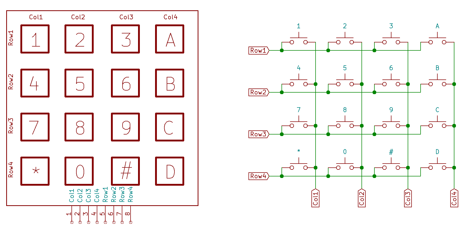
The schematic for the keypad matrix you will use for this lab experiment is shown above.
3.3 Driving multiplexed displays
A 7-segment display is one that has seven LED segments in the shape of a number “8”. By selectively turning segments on, other numbers can be displayed. In practice, such displays have more than seven segments. An eighth segment shows a decimal point. Recall Figure 2, from ECE 270, that shows the names of the segments of a display. The top segment is customarily called “A”. Proceeding clockwise, the next ones are named “B”, “C”, and so on. The middle segment is named “G”. The decimal point is named “DP”.
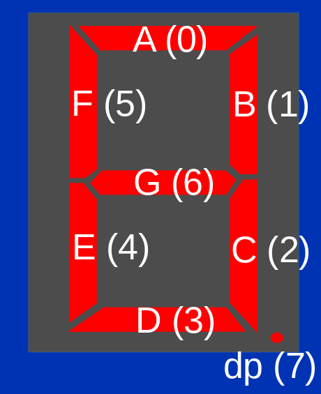
For this lab experiment, you will be using the TDCR1050M 4-digit 7-segment LED display. This device was made to be used in a clock, so it has a middle colon for use in displaying a time. Another dot on the display can be illuminated to indicate things like an alarm setting. For this experiment, we will use only the digits and decimal points.
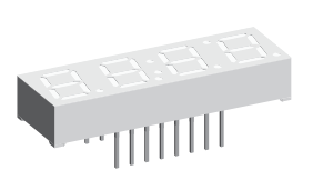
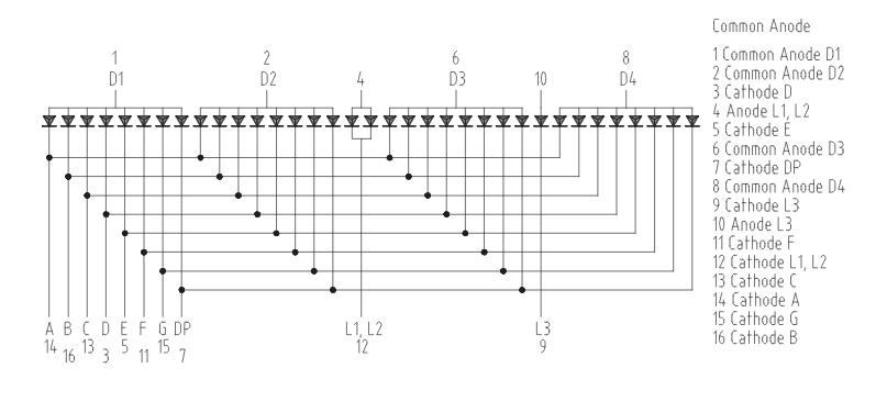
If you look at a picture of the physical device in figure above, you see that it has only two rows of eight pins on each side. Only sixteen pins are used to control more than 30 individual LED segments that must be independently lit to form four distinct digits and decimal points. To do so, it uses a “common anode” configuration so that one pin is connected to the anodes of all the LEDs on one digit. There are four distinct pins connected to the anodes of the four digits. There are another eight pins connected to similar cathodes on all the displays. For instance, one pin is connected to the four “A” cathodes on the four digits. This means it is possible to illuminate all four of the “A” segments on the four digits by applying a positive voltage to the four common anodes and a negative voltage to the pin connected to all of the “A” segments. It is not possible to simultaneously illuminate the “A” segment of all the displays and illuminate the “B” segment of only a single display. Figure below shows the schematic for the connections to all of the LED segments for the display.
If it is not possible to independently turn on and off individual segments at the same time, how is it possible to display distinct numerals on the four groups of segments? This display is made to be multiplexed. In a manner similar to how we cannot detect the exact moment that a button in a matrix is pressed, we cannot simultaneously turn on every LED segment we need. Instead, the segments of the first digit are turned on, then the segments of the next digit are turned on, then the third, then the fourth. If each individual digit is illuminated for one second, then the display will not be perceived as a four-digit number. If, however, the cycling through the digits is done quickly enough, it will appear that all of the numbers are shown simultaneously. This is because of the human eye’s persistence of vision. A flickering light—as long as the flickering is rapid enough—is perceived as continually on, although maybe dimmer than normal.
As an example, consider the result of applying the following cycle of voltages applied to the pins of the display:
- A positive voltage to pin 1 (D1), and a negative voltage to pins 16 (B) and 13 (C)
- A positive voltage to pin 2 (D2), and a negative voltage to pins 14 (A), 16 (B), 3 (D), 5 (E), and 15 (G)
- A positive voltage to pin 6 (D3), and a negative voltage to pins 14 (A), 16 (B), 13 (C), 3 (D), and 15 (G)
- A positive voltage to pin 8 (D4), and a negative voltage to pins 16 (B), 13 (C), 11 (F), and 15 (G).
When these four configurations are applied repeatedly and at high speed, it will appear that the four-digit number “1234” is present on the display.
How rapidly must you cycle through each digit to achieve the effect of persistence of vision? Usually, anything flickering faster than 30 times per second appears to be continually on. As long as all of the digits of the display are turned on and off more than 30 times per second (even though none of them are on at the same time as others) the display will appear continuous. In this lab experiment, you will use two groups of the four-digit displays (eight digits in total), and you will turn on each digit for one thousandth of a second. By illuminating each individual digit for one-thousandth of a second, any one of the eight displays will be illuminated eight times less frequently (or 1/125th of a second). This is much faster than is needed to perceive the digits as all being on simultaneously.
3.4 Use of a sink driver and high-side transistors
Most students, when they approach the idea of multiplexing, would be more comfortable with a “common cathode” display instead since it could be configured so that a positive voltage applied to the pin connected to the anodes of all “A” segments would illuminate that segment when a negative voltage is applied to the pin connected to all the cathodes of the digit. If you were connecting the pins directly to your microcontroller, that might even make sense. Nevertheless, the current-flow requirements for the LEDs make it impractical to illuminate many of them using only the capabilities of the microcontroller. Instead, it is common use sink driver connected to the cathodes of each type of segment (e.g., “A”, “B”, “C”, etc…). A sink driver is a device that is capable of sinking (connecting to ground) a connection with a large current flow. 47Ω limiting resistors will be placed in between the sink driver and each cathode to prevent too much current from flowing through each segment. Conveniently, the sink driver will sink current through an output pin when its corresponding input pin is high. In this way, it acts as an open-drain inverter. (A sink driver cannot push an output pin high.) Using the sink driver, a logic high applied to the driver will cause the particular segment to illuminate, which is how you would like to think about it.
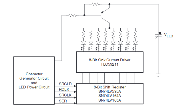
Consider the circuit in the figure above that appears in the TLC59211 datasheet. In this lab experiment, you will wire the microcontroller to the sink driver rather than an 8-bit shift register. The device at the top of the diagram is a PNP bipolar junction transistor (BJT). This device will conduct current through the top pin (the emitter) in the direction of the arrow, and out the bottom pin (the collector) when the middle left pin (the base) has a voltage lower than the emitter (and a small current coming out of it). It is conceptually similar to a P-Channel MOSFET except that a MOSFET does not require a substantial current flow through its gate. By contrast, the collector current for a BJT is directly proportional to its base current.
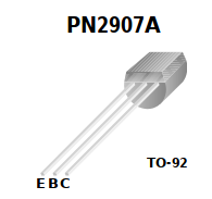
You will use one PN2907A PNP BJT (in a TO-92 package) for each anode of each digit of the display. Pay careful attention to the designations for the pins (E,B,C for emitter, base, collector) on the device:
- Pin 1 is the emitter
- Pin 2—in the middle—is the base,
- Pin 3 is the collector.
The anode of a digit must be able to supply enough current for all eight segments of the digit simultaneously. The datasheet for the TDCR1050M shows that each of the eight segments of each digit could use as much as 25 mA, although you won’t have that much current flow for this experiment. A microcontroller pin would not be able to supply enough current to illuminate all of the segments of a digit, but a PN2907 transistor will provide at least 200mA if needed. Because the transistor is driving the positive voltage to the display, it is referred to as the “high-side” driver for the display. You may think of the sink driver as the “low-side” driver for the display.
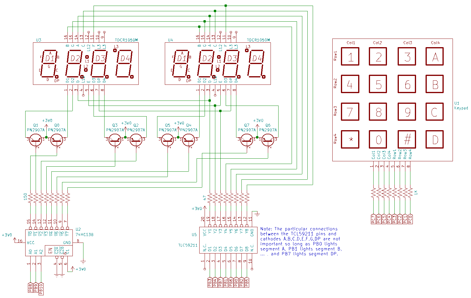
Rather than try to deal with low voltage to enable current flow through each PNP transistor, we will add one more device: a 3-to-8 decoder with active-low outputs. Three input pins select one of eight outputs to be driven low. Each one of these outputs will be connected, through a series resistor, to the base of one high-side driver transistor. Altogether, eleven pins of the microcontroller will be used to drive the display: three to select the digit to turn on through the decoder and high-side driver transistors, and eight more to turn on the segments of the selected digit. A full schematic of the wiring for the display and keypad is shown in figure below.
3.5 Tips for wiring the circuit
- NOTE : You do not need to follow this exact form. You can wire it in a way that makes sense to you, but you must keep it neat.
You’ll be assembling two 4-digit display modules, driven by 8 PN2970A transistors, a TLC59211 sink driver, 8 resistors between the sink driver and LED cathodes, a 3-to-8 decoder, and 8 more resistors between the decoder and the transistors. Another eight resistors will be used to connect the keypad to the microcontroller. With some planning, it will be possible to assemble this quickly and reliably. Here are several suggestions to make it as easy as possible…
3.5.1 Place the transistors next to the displays
The collector of a PN2907A transistor must be connected to each of pins 1, 2, 6, and 8 of both display modules. Notice that these pins are all on one side of the display, and that two of them are near the ends of the row of pins. There are no connections to the left or right of the connector, but there is a lot of space taken up by the displays. Rather than run long wires from the transistors to the displays, put the collector of one transistor on pin 1 and the collector of another transistor on pin 8. The other pins of each transistor are placed to the left and right, respectively. Add another two transistors further out by combining the emitters on the same breadboard row. Finally, connect the collectors of the outermost transistors to pins 2 and 6. Looking from left to right, the first backward-facing transitor will connect power to D2 (pin 2). The next forward-facing transistor will connect power to D1 (pin 1). The next transistor will connect power to D4 (pin 8), and the fourth transistor will connect power to D3 (pin 6). Note the alternating backward-facing, forward-facing manner in which the transistors are placed. The base (middle pin) of each of the transistors is what will be driven, through a 150Ω resistor, by the decoder.
3.5.2 Wire the resistors to the display
Leave some space on the right side of the rightmost display module, connect the resistors on the top side of the display module, and run wires from the other side of the resistors to the TLC59211. Neatness of connections will avoid a great deal of problems when you reach the point of debugging. A maze of wires that loop far over the breadboard will not only block the LED segments, it will be difficult to diagnose, and be prone to damage when the wires are snagged on objects while in transport.
3.5.3 Chain the cathodes from one display to the other
The eight connections to the cathodes of display on the right should be made to the same eight pins on the display on the left. Use eight wires to connect them together. I.e., connect pin 16 on the left display to pin 16 of the right display, pin 15 to 15, etc. The pins to connect together on the top side of the displays are 16, 15, 14, 13, and 11. The pins on the bottom side of the displays are 3, 5, and 7.
3.5.4 Connect resistors to the decoder
The 150Ω resistors should be placed directly on the 74HC138 decoder. If you want to be tidy, you might cut the leads to minimize the amount that they stick out of the breadboard. If you do so, make sure that leads of every resistor is wide enough to span four breadboard holes. A width of only three would mean, for instance, that the resistor on the Y2 output would connect to the VCC pin of the chip. Wires should be run from the other ends of the resistors to the bases of the transistors. Connect output Y0 through a 150Ω resistor to the base of the PNP transistor connected to pin 1 of the left display. Note that output Y7 is on the bottom side of the 74HC138 decoder on pin 7. Pin 8 is the ground connection. The decoder’s select lines, A0, A1, and A2 (pins 1,2, and 3, respectively) should be connected to PB8, PB9, and PB10. Pins 4, 5, and 6 should be connected to GND, GND, and VCC, respectively. These three pins are the enable pins for the decoder. Unless all three of these pins are enabled, none of the decoder outputs will be asserted (driven low).
3.5.5 Check your wiring
Use the check_wiring test in the autotest menu or uncomment the call to check_wiring() in main(). When first started, the digits 01234567 should appear on the seven-segment displays. The decimal point on the leftmost digit should illuminate for 0.25 seconds, then turn off and the decimal point on the next digit should illuminate for 0.25 seconds. The decimal point should cycle through all of the digits in two seconds and continue again with the leftmost.
As the decimal point illuminates, make sure that the other segments of each digit remain at the same brightness. If the other segments of a digit grow dimmer, it may be that the driver transistor for that digit is backward. A BJT transistor normally amplifies a small base-emitter current with a large collector-emitter current, but a BJT can also work backward so that it amplifies a small base-collector current to a larger emitter-collector current. The amplification is not as high, and it limits the current provided to a digit. The more segments per digit are lit, the dimmer they are. Carefully note the orientation of the transistors connected to the D1, D2, D3, and pins of each display.
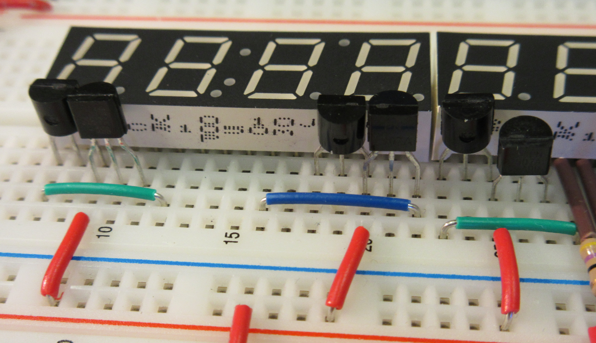
3.5.6 Example Breadboard
Ignore the LCD in the lower right-hand corner.
(100 points) 4. Experiment
Download the lab 7 template project from lab website. Make sure to configure the debugger as in previous labs.
(20 points) 4.1 The basics
(5 points) 4.1.1 enable_ports: Enable GPIO ports
Implement the function enable_ports() that does the following:
- Enables the RCC clock to
GPIOBandGPIOCwithout affecting any other RCC clock settings for other peripherals - Configures pins PB0 – PB10 to be outputs
- Configures pins PC4 – PC8 to be outputs
- Configures pins PC0 – PC3 to be inputs
- Configures pins PC0 – PC3 to be internally pulled low
As usual, you should not alter the configuration for any other pins. For instance, if you were to improperly alter the MODER setting for PC12, the serial port would stop working.
(5 points) 4.1.2: Basic Interrupt Service Routine (ISR)
Write an interrupt service routine (ISR) for Timer 6 (TIM6). Look up the exact name of the ISR in startup/startup_stm32.s and copy it into the recommended spot in your main.c. (Yes, it has a long, strange name that you will understand the reasons for later.) It should do the following things:
- Normal ISRs must acknowledge an interrupt so that it will not be immediately reinvoked. To acknowledge a basic timer interrupt, you must write a zero to the
UIFbit of the status register (SR) of the timer. Sometimes, interrupts must be acknowledged by writing a ‘1’ bit as you saw for theEXTIsubsystem. In this case, you write a ‘0’ bit to theUIFbit to clear it, and write all other bits to ‘1’ to avoid clearing anything else. In other words, you write the bitwise inverse ofTIM_SR_UIF, which is~TIM_SR_UIF. There will be no other bits set in theTIM6_SRregister, so you may simply write 16 bits of zeros to theTIM6_SRregister. It will do what you need and not cause any other problems. Be prepared to be more selective with peripheral status registers in future lab experiments. - Toggle the PC8 bit. To do so, you should check the current value of bit 8 of the
ODR. If it is set, use theBRRregister to turn it off. Otherwise, use theBSRRregister to turn it on. Avoid writing directly to theODR. Multiple ISRs will modify pins ofGPIOC, so it is important to use atomic operations.
This is the simplest way that you can demonstrate any timer: Write the simplest possible ISR, and blink one LED.
(10 points) 4.1.3: setup_tim6: Configure a basic timer
Now that you have written a simple ISR for the Timer 6 interrupt, you can configure timer 6 to invoke that interrupt. Write a subroutine named setup_tim6 that does the following: (See the lecture notes for an example.)
- Enables the RCC clock to Timer 6. It is up to you to determine how to do so. You might look at Section 7.4 of the Family Reference Manual to find which bits of which register (usually, one of
AHBENR,APB1ENR, orAPB2ENR) to set. You can also look it up in the I/O Register browser in SystemWorkbench. - Configure
TIM6_PSCto prescale the system clock by48000. (You should know, by now, that you should not write the value 48000 to the PSC register to do this.) This will divide the 48 MHz system clock by 48000 to send a 1 kHz clock to the free-running counter of the timer. - Configure the Timer 6 auto-reload register (
TIM6_ARR) to have a counting period of 500. With an input clock of 1 kHz, this will cause a timer update event to occur every 0.5 seconds. Since we intend to raise an interrupt that will run the ISR you just wrote, it will cause the PC6 LED to toggle every 0.5 seconds (or blink at a rate of 2 Hz). - Configure the Timer 6 DMA/Interrupt Enable Register (
TIM6_DIER) to enable the UIE flag (use the symbolTIM_DIER_UIEfor this). This will enable an update interrupt to occur each time the free-running counter of the timer reaches the ARR value and starts back at zero. - Enable Timer 6 to start counting by setting the CEN bit in the Timer 6 Control Register 1. (Set
TIM_CR1_CENinTIM6_CR1.) - Enable the interrupt for Timer 6 in the
NVIC ISERin a manner similar to how you did in lab 6.
Once you complete this subroutine and run it, you will see the PC8 (Green) LED blink at a rate of 1 Hz.
(20 points) 4.2 A display multiplexing and key scanning application
Once you’ve successfully written a timer ISR, more interesting applications are easy to implement. Rather than add them to the ISR you just wrote, you’ll write an ISR for a second timer and a configuration subroutine that will turn off Timer 6. This will allow the code you just wrote to be tested independently.
The application to be built for this lab is the lunar lander game that you may have seen in ECE 270. You will use the concepts for this system, as well as the hardware it uses, for future lab experiments.
4.2.1 Data structures for the application
Three very simple global “data structures” will be used to keep track of the values needed for this application. They are already defined at the top of the main.c template file.
colis a single-byte integer, with a value ranging from 0 – 7, that indicates the digit presently being displayed. AND the lower two bits indicate the row that is being scanned. For purposes of these subroutines, digits will be numbered, left-to-right 0 – 7, and keypad columns will be numbered, right-to-left 0 – 3. For instance, if the value ofcolis 6, that would mean that digit 6 (second from the right) is illuminated, and that column 2 (containing buttons 2, 5, 8, and 0) is being scanned.dispis a 9-entry array of single-byte values, each of which represent the characters to display for each digit. The entries for this array should be pre-initialized to the following values"Hello..."- This string will be shown on the seven-segment displays on startup.
- You might be saying “I only count eight characters there. Why do you say nine?” Remember that every string is terminated by a NUL (zero) byte. If you write a quoted string with eight characters in it, nine bytes of space are allocated. This will be important for us when we write messages into the string with
sprintf.
modeis a one-byte value that determines what information is to be shown on the seven segment displays. We’ll store a character value here to help us remember what the mode means.thrustis a one-byte value that indicates the last specified throttle setting. It will always have a numeric value of 0 to 9.fuelis a two-byte (halfword) value that indicates the remaining amount of fuel for the lunar lander. It is initialized with the value 800 (decimal).altis a two-byte (halfword) value that indicates how far about the lunar surface the lander is. It is initialized with the value 4500 (decimal).velois a two-byte (halfword) value that indicates the current velocity of the lander. We choose to represent velocities that decrease altitude as negative values. Since the lander is falling toward the lunar surface, the value ofvelowill normally be negative. The initial value ofvelois zero. Gravity will gradually make it negative.
These variables are created and initialized at the top of your main.c file.
(10 points) 4.2.2 show_char: Display a single character
Implement the function show_char that will select a digit to light using PB8, PB9, and PB10 and also output the 8-bit pattern to display on that digit on PB0 – PB7. A table provided for you gives the mapping from the character number to the segments of the LEDs to illuminate. Such a data structure could arguably be called a font since it shows the elements of the data to display. You can call it exactly that. The font array is in read-only memory (i.e., in the text segment). It includes most of the printable ASCII character set, although some characters are not possible on a 7-segment LED (e.g., “m” and “w”).
To implement the subroutine, the pattern should be read from the nth element of the font array. Since all of the Port B output pins are being used for the display, you may simply output the combined value to the ODR. Note that, as a defensive coding practice, you should ensure that the offset value is in the range of 0 – 7.
void show_char(int n, char c) {
    make sure 0 <= n <= 7, i.e. lies in the valid range
    // font[c] contains the bit setting for PB0-7 (the sink driver)
    write content of font[c] to the corresponding bits in `GPIOB->ODR` (i.e. those pins controlling the decoder and the sink driver)
}
4.2.2.1 fill_alpha: Show sequential letters
Once you implement show_char, you may uncomment the call to fill_alpha, which is provided for you. It will call show_char with the values ‘A’ through ‘H’ to show the series on the display. You may use this for debugging. Once it is working, show your TA to confirm that you have completed this much of the lab experiment. You will not receive credit for the remainder of the lab if you cannot demonstrate this much in lab.
(10 points) 4.2.3 drive_column: Update the keypad column being scanned
Implement the function drive_column(int c) that updates the column of the keypad that has a logic high applied to it. Remember that the column being scanned is the least two significant bits of the col variable (since we just have 4 columns). Not all of the pins of Port C configured for output are used for the same thing. One of them is for blinking PC8. You should not simply write to the ODR to implement this subroutine. Use the BSRR register to update only the bits 4 – 7:
void drive_column(int c) {
    c = least 2 bits of c
    first clear the bits 4-7 of GPIOC
    then set the bits corresponding to the column `c`
}
Remember that the upper 16 bits of BSRR clear pins and the lower 16 bit set pins. Setting takes precedence over clearing.
(20 points) 4.3 Implement keypad scanning and building a game
For the next three substeps, you will implement keypad scanning.
(5 points) 4.3.1 read_rows: Read the row values
Implement the following function to examine the IDR of Port C and return the 4-bit reading of the rows of the keypad.
int read_rows() {
    return the 4-bit reading of the rows
}
(10 points) 4.3.2 rows_to_key: Translate row of a column to a key
Implement the following function that examines the rows reading for a particular column and turns it into a character. Remember that only the lower two bits of the col determine the column. We want to turn the row/column combination into a number and then use that number as the offset into an array called the keymap_arr that is initialized for you in main.c.
The keypad columns are scanned from right-to-left, where the rightmost column is column 0 and the leftmost column is column 3. Rows are interpreted from bottom-to-top.
Buttons:                 Offsets:
+---+---+---+---+        +---+---+---+---+
| 1 | 2 | 3 | A |        | f | b | 7 | 3 |
+---+---+---+---+        +---+---+---+---+
| 4 | 5 | 6 | B |        | e | a | 6 | 2 |
+---+---+---+---+        +---+---+---+---+
| 7 | 8 | 9 | C |        | d | 9 | 5 | 1 |
+---+---+---+---+        +---+---+---+---+
| * | 0 | # | D |        | c | 8 | 4 | 0 |
+---+---+---+---+        +---+---+---+---+
For instance, if the ‘8’ button is pressed, the number for that button should be 0x9 (an offset of one from the start of column 2: 2*4 + 1 = 9). When the ‘*’ button is pressed, the offset should be 12 (hexadcimal 0xc) since it is in column 3, row 0 (3*4 + 0 = 12).
The function to implement is:
char rows_to_key(int rows) {
    compute the offset of the button being pressed right now from `rows` and `col`
    // Note `rows` will be a 4bit value from reading the IDR register of the row pins of the keypad
    lookup `c` in the `keymap_arr` indexed by the offset
    return c;
}
(5 points) 4.3.3 handle_key: Do something for a particular key
Implement the following function that decides what to do for a key passed as an argument. The function to implement is:
void handle_key(char key) {
    if key == 'A'/'B'/'D', set mode to key
    else if key is a digit, set thrust to the represented value of key, i.e. if key == '1', thrust = 1, not '1'
}
(20 points) 4.4 Timer 7
(10 points) 4.4.1 Timer 7 ISR
Write an ISR for timer 7. You should look up the exact name for it in startup/startup_stm32.s. The ISR should first acknowledge the timer interrupt (similar to what you did for the timer 6 ISR). Then, it should do the following things to invoke the functions you just wrote:
acknowledge the interrupt first
read the row values
if rows != 0 {
    convert it to key
    then handle with `handle_key`
}
Get character from the `disp` string at position `col`
show the character at column `col`
increment col by 1, remember to wrap it around if it is > 7
drive the new column
The reason we do not drive column and then immediately read rows is because it sometimes takes a little time for current to flow into the row of buttons and settle out to be read properly on the input pins. It doesn’t always happen, but when students energize the column and immediately try to read the rows, and it doesn’t work, then it’s a Bad Day ™.
(10 points) 4.4.2 setup_tim7: Configure timer 7
Write a subroutine to enable and configure timer 7. This will be similar to the subroutine you wrote to configure timer 6. Remember that timer 6 was written as a simple test, and it interferes with everything you’ve written since then (because it updates PC6). This is the point where you must disable timer 6. Here are the things you need to do:
- Enable the RCC clock for TIM7.
- Set the Prescaler and Auto-Reload Register to result in a timer update event exactly once per millisecond. (i.e., a frequency of 1 kHz)
- Enable the
UIEbit in theDIER. - Enable the Timer 7 interrupt in the
NVIC ISER. - Set the
CENbit inTIM7_CR1
Note: A mistake made by students is to set the TIM7_ARR register to zero. When you do that, the timer won’t do anything. That’s worth a bigger warning…
Once you are done with this function, uncomment the call to it in the main().
Debugging tip: It is often helpful to slow down the rate of interrupts to human speed to better understand what is going on. For instance, if you set the timer 7 rate to one interrupt per second, you’ll be able to see exactly what is happening. You should see individual digits displayed for one second at a time on the LED displays. You’ll be able to press buttons at exactly the right time to be detected by
read_rows.
(20 points) 4.5 Game state updation
(5 points) 4.5.1 write_display: Write a formatted message on the display
The subroutines written above will be used to show characters on the display and scan the keypad. They are called by the timer 7 ISR. Any update to the disp array will be immediately copied to the 7-segment LEDs a thousand times per second.
So far, there is nothing to interpret or use the keypad events to change the display. It just says “Hello…” Now, you will write a function called write_display that will check the mode variable, and write a message into the disp array based on the selected mode. For instance, when we press the ‘A’ key, the display should show the altitude. When we press the ‘B’ key, it should show the current fuel level. When we press the ‘D’ key, it should show the speed of descent. If we make a soft landing, the display should show “Landed” and if we make a hard landing, it should display “Crashed”.
To update the disp array, we will use the snprintf library function that is provided in the standard peripheral library. That will allow us to easily turn integer values into character strings.
The subroutine to implement is as follows:
void write_display(void) {
    if mode == 'C'
        update `disp` to be "Crashed" (without the double quotes of course)
    if mode == 'L'
        update `disp` to be "Landed " (Note the space)
    if mode == 'A'
        update `disp` to be the string produced by printf("ALt%5d", alt)
    if mode == 'B'
        update `disp` to be the string produced by printf("FUEL %3d", fuel)
    if mode == 'D'
        update `disp` to be the string produced by printf("Spd %4d", velo)
}
Each time write_display is called, it will overwrite the previous contents of the disp array. The code invoked by the timer 7 interrupt will copy it to the 7-segment displays.
(5 points) 4.5.2 update_variables: Compute altitude, velocity, and acceleration
Implement a function void update_variables(void) to update the variables that describe the lunar lander. First the code. Then an explanation:
void update_variables(void) {
    `fuel` decrement by `thrust` amount
    if (fuel <= 0) {
        set `thrust` and `fuel` to 0
    }

    increment `alt` by `velo` amount
    if (alt <= 0) { // we've reached the surface
        check if `-velo` < 10
            then:
                mode = 'L'
            else:
                mode = 'C'
        return;
    }

    increment `velo` by `thrust - 5`
}
This subroutine will be called periodically. For each time period, an amount of fuel determined by the thrust is deducted from the fuel supply. When the fuel reaches zero (or less), there can be no more thrust, so the thrust and the fuel level are set to zero.
Each time this subroutine is called, the current velocity (velo) is added to the altitude (alt). You can think of this as a form of discrete integration. Velocity is the derivative of distance per unit of time. Distance is the summation of velocity over time.
If the altitude is zero (or less), we’ve reached the lunar surface. We have to check the velocity to determine what kind of landing it was. If the speed was less than 10, we’ll consider it a successful landing. Otherwise, we’ll consider it to be a crash landing. Remember that the velocity will be negative at the time of a landing, so we need to negate when we compare it to 10. Once landed/crashed, we do not want to make further veclocity calculations, so the subroutine should return.
Finally, the new velocity (velo) will the the summation of the accelerating forces on the lander. Here, we’ll integrate those forces. The summed velocity will change by adding the thrust and subtracting the gravity (5).
These calculations are all that are needed to determine the motion of the lander. Note that we’ve deliberately avoided declaring units for any of the quantities we’ve described. You can feel free to imagine that the velocity is meters per second, feet per minute, furlongs per fortnight, or any other metric you prefer. The dimensions are not important so long as we have a playable game.
(10 points) 4.5.3 Set up timer 14
To periodically invoke update_variables and write_display, create an ISR for timer 14. In it, do the following:
void ISR(void) {
    Acknowledge the interrupt
    call update_variables();
    call write_display();
}
And then implement the function setup_tim14 to initialize Timer 14 to invoke an update interrupt twice per second (2 Hz).
At this point, you should have a playable game.
3. Playing the game
This university has a long history of producing graduates who are able land on the moon. Once your program works, you may want a strategy to be equally successful. Here is one:
- When the program starts, the altitude is 4500, and the thrust is zero, so the lander goes into a free fall. Continue to monitor the altitude.
- The moment the altitude drops to 3000, press ‘8’ to slow the descent.
- Press ‘D’ to monitor the rate of descent. The speed shown should reduce in magnitude from -119. When it is less than -10, press ‘5’ so that the thrust matches the force of gravity. The velocity will remain the same for the remainder of the descent.
- Press ‘A’ again to watch the altitude. There should be enough remaining fuel to have a controlled descent and soft landing.