f2022-public-labs
Lab 1: General Purpose I/O
In this experiment, you will learn how to connect simple input devices (push buttons and keypad) and simple output devices (LEDs) to an STM32 development board. You will learn how to configure the General Purpose Input/Output (GPIO) subsystems. You will read values from and write values to these pins.
NOTE: Past this point, if you use hexadecimal or binary code, you should comment each line so we can see what you’re intending to do. If it’s in CMSIS, it does not require a comment.
NOTE: Past this point, wiring good practice rules are in effect. Please see the Brightspace resource on it. If your breadboard is not neat and not working, we will not help you to get it working.
NOTE: Past this point, the 20-minute rule is in effect.
2. Instructional Objectives
- Connect LEDs and push buttons/keypad to the STM32 GPIO pins.
- Configure the GPIO subsystems.
- Read values from and write values to the GPIO pins.
3. Background
By default, every subsystem in a microcontroller is disabled in order to reduce power consumption, and the GPIO subsystem is no exception. Each port must first be enabled by turning on a clock for the port controller. Only after that, can the port be configured. The following two steps are needed to configure I/O pins for use:
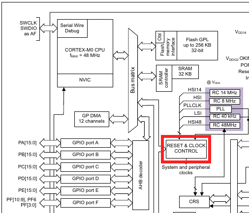
First, the Reset & Clock Control (RCC) subsystem must be configured to enable a GPIO port for use. This is done by turning on the specific bit in the AHBENR (Advanced High-Performance Bus Enable Register). In doing so, be sure not to turn OFF important bits such as the SRAMEN bit. Use your lecture notes to determine how to do this. For this lab, in particular, you should enable Ports B and C by ORing the appropriate values into the AHBENR register. A figure of the reset and clock control is shown below:
Second, an enabled port must have its pins configured as either inputs or outputs (or some other functions that we will use in future labs). For this lab, we will initially use Port B pins as inputs and Port C pins as outputs. For instance, the inputs used will be pins PB3 and PB4 (pins 3 and 4 of Port B). For both ports there are some pins whose function you should not modify. In particular, you should not change PA13, PA14, PC14, or PC15 since these are used for an External Oscillator, Debugging, and Programming interfaces. Instead, use code from your lecture notes to learn how to set and clear only the bits you want without altering other bits.
A functional diagram for an STM32F0 GPIO port is shown below:
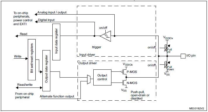
In this experiment, you will enable general purpose (digital) inputs and outputs. That will involve using the input data register (IDR) and output data register (ODR) for each port. We will consider analog inputs and outputs in future lab experiments.
4. Experiment
You should start by downloading the Lab 5 student template from the Lab website and import it into System Workbench. Since both the ARM DS and the System Workbench are based on eclipse, you can follow the same approach to import the template.
Every subsection of this step (4.1, 4.2, …, etc) requires a checkoff by your TA. Do NOT wait until the end of lab to check everything off.
To prepare for debugging, make sure you follow the steps in lab 0.1 to set up the debugger properly.
In addition, a precompiled autotest object has been incorporated into the template folder. You can utilize it to test both the wire connection and subroutines. To do so, make sure you have connect the UART serial adapter and the STLink to the microcontroller. Then you will need to uncomment the line autotest() in the main.c file and start the debugging on System Workbench. After the debugger successfully launched, make sure it goes into the autotest() and launch a serial connection to the microcontroller in a terminal with screen /dev/ttyUSB0 115200 (the same one in lab 0.1). You should see a prompt similar to the following:
Spring 2022 tests for lab 3.  Type 'help' to learn commands.

>
You can then type help to proceed the testing. You will use this to demo your implementation and wiring to the TAs.
4.1 (15 points) Configuring Port B
Using the main.c template file provided for this lab, fill in the C procedure for initb. This is should enable the RCC clock for Port B, set pins PB8-PB11 as outputs and set pins PB0 & PB4 as inputs. Please refer to the notes for a refresher on how this is done. This should be done without disabling other pins in RCC such as SRAMEN, configuring other pins as outputs, etc. Only the bits needed to complete the required configuration should be changed.
The global variable RCC is provided for you to use as the base address for the Reset and Clock Control I/O registers. Use the global variable RCC->AHBENR to access the AHBENR I/O register. In addition, the enable values are also predefined as well. For instance, you can use RCC_AHBENR_GPIOBEN as a constant to enable the GPIOB bit in the AHBENR register. Most of these symbols should have the same names as in the family microcontroller manual. To use the symbols, make sure you have use the stdperiphlib when creating the project to use the provided template, then just type in the exact words for these symbols. Also you can use CTRL + Space to autocomplete these symbols in SystemWorkbench,
Similarly, the global variable GPIOB is provided along with the symbols for MODER, IDR, ODR, BSRR, etc. Use these in a similar manner to RCC and AHBENR (i.e. GPIOB->MODER will access the MODER reg for GPIO port B) to configure pins PB8-PB11 as output pins (and to read and write their driven values in later sections.)
If you look at the documentation in the Family Reference Manual regarding a GPIO port’s MODER register, you will notice that all pins that can be used as inputs are set as inputs by default. We want you to get some practice clearing bits of the MODER as well as setting bits. Your subroutine should also configure pins 0 and 4 of Port B as inputs with the assumption that they may have already been configured as outputs. This means you should clear the two-bit value for each pin in question to 00.
The autotest module provided for you will call this and every other subroutine you write multiple times in different ways. It will deliberately set and clear other bits in the AHBENR to make sure that you are doing a proper OR operation to set only the necessary bits and not setting or clearing any other bits. The procedure for ORing bits into a configuration register may seem cumbersome, but it will occur repeatedly for many types of peripherals. You’ll soon get used to it.
When debugging individual subroutines you should leave the call to autotest commented out so that you can step through the operation of each subroutine. You must complete each step of implementation in sequence. You will not get credit for steps 2 through 6 without first satisfactorily completing step 1.
Hint: When debugging your code, you may consult the “I/O Registers” tab in the Monitor window. This tab provides a hierarchical listing of all of the various peripherals utilized by the microcontroller and their sub-registers. By default their values are not shown; double clicking on a given entry will cause the debugger to track the values of that entry and its lower elements. Use this to confirm that the various registers you are writing to are taking on the values which you expect. An example of this is shown below. When you cannot understand why a GPIO port is behaving as you expect, take a look at the registers and make sure their contents are being set correctly. This is a process that you will use for the rest of the semester.
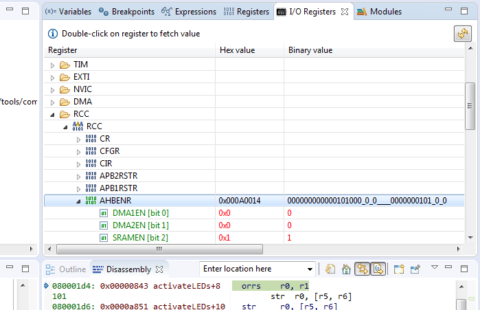
You can also use the I/O Registers viewer to modify values to experiment with register settings. As you progress through the lab experiment, you will find that you can use the I/O Registers viewer to deposit values into the ODR of Port C. This will cause LEDs to illuminate. You can also examine the value of the Port B IDR in real time to determine if a button is pressed. Note that the same rules apply just as if you wrote code to do things programmatically. You will not be able to view or adjust values for any of the registers of a GPIO port before enabling the clock to that subsystem in the RCC AHBENR. You can experiment with doing that manually as well.
4.2 (15 points) Configuring Port C
For this section, you will need to complete the subroutine initc in main.c so that GPIOC’s clock is enabled in RCC and it configures only pins 4, 5, 6 and 7 of Port C as outputs. These pins will drive the colunms of the keypad (the wiring and schematic for which will be introduced later). Set pins 0, 1, 2, and 3 as inputs and to use the internal pull down resistors by setting the relevant bits in the PUPDR register. These will read the rows of the keypad and need to be pulled down to keep from reading erroneous floating signals. You should use the symbolic constant GPIOC to access registers of GPIO port C. Similar to GPIOB, you can use GPIOC->MODER and GPIOC->PUPDR to access the mode register and the pull-up/down register for port C.
Reminder: Be sure not to change the configuration for pins 13, 14, and 15.
4.3 (15 points) Set PORTB pin outputs
For this section, you will need to complete the subroutines setn in main.c. The first parameter is the bit number (the same as the pin number) to be set (by setn). The second parameter is the value to set the pin to (either zero or anything not zero). The setn subroutine turns off the pin/bit number in the GPIOB_ODR register if the value in the second parameter is zero. Otherwise, it turns on the pin/bit number. For instance, if you execute setn(8, 0), it would turn pin 8 off. If you invoked it as setn(8, 59823) it would turn pin 8 on. Here, the value 59823 is arbitrary. Any value other zero in the second argument should turn the pin on. Use the variable GPIOB->ODR to ACCESS the output data register. You are encouraged to use the BRR and BSRR registers to implement these subroutines.
4.4 (15 points) Read PORTB pin inputs
Complete the subroutine readpin in main.c. This function accepts a bit number as parameter 1. It returns the value in GPIOB_IDR at the bit specified by parameter 1. In other words, the subroutine should return 0x1 if the pin is high or 0x0 if the pin is low.
4.5 (0 points) Wiring LEDs, Push Buttons, and Keypad
Before You Proceed:
Unplug the programmer the USB port to remove power from the development board before you wire components. Anytime you plug things in to the microcontroller when the power is on, you run the risk of connecting something you shouldn’t have and causing damage. By removing power, you have the opportunity to double-check your work before you reconnect power. You can ask one of your TAs to triple-check your work.
After you remove the power from your development board, wire your circuit as shown below. Ensure that you are connecting resistors for the buttons to the 3V power. You are advised to connect the power buses on your breadboard array to the GND and 3V connections on the development board. (Leave the 5V pins unconnected to avoid using them.)
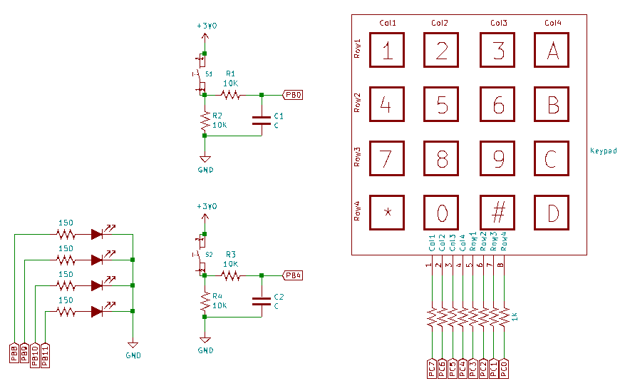
Use your choice of red, yellow, and green LEDs to build the circuit above. To determine the orientation of an LED, look at the length of the leads. The long lead of the LED is usually the anode (the positive terminal) and the short lead is the cathode (the side connected to ground in the schematic). You can also search for a flattened section of the circular rim of the LED. That also indicates the cathode.
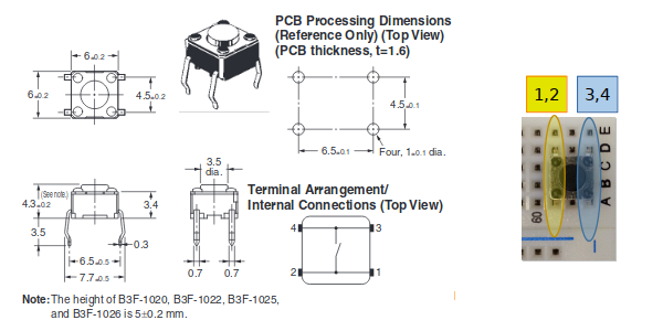
Use four-lead “tactile” push buttons for the switches. The 6x6mm push buttons work the same way as the 12x12mm push buttons. Note that pins 1 and 2 are connected together internally as well are pins 3 and 4. The push button is “normally open”. When it is pressed, pins 1 and 2 are connected to pins 3 and 4. See the diagrams below for more details.
You will use a 16-button keypad for this lab experiment. One configuration for such an arrangement of buttons would be to have two wires for each button (32 wires total) so that each button could be independently monitored. That would require a lot of pins on the keypad which might make it difficult to use on a breadboard. An optimization might be to have one common power connector and one more connector per button (17 wires total) so that each button could still be monitored individually. But this is still too many pins on the keypad than manufacturers will usually support, and the numbers would only be much worse for keypads with even more buttons.
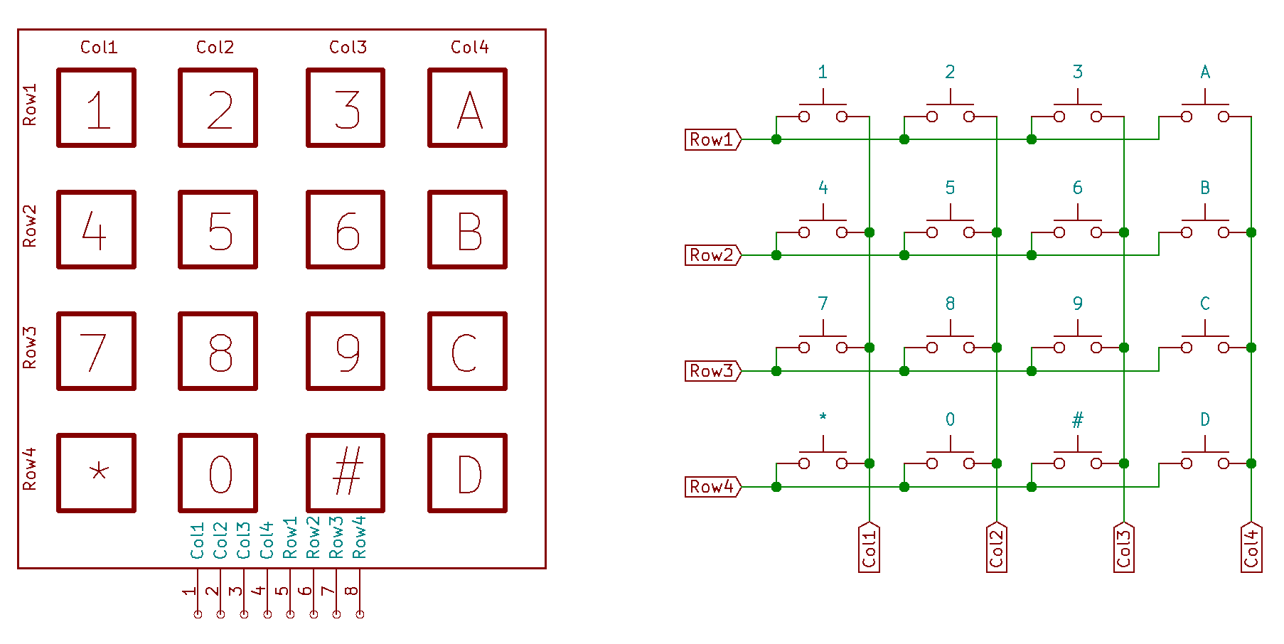
The typical concession for keypads is to have multiple common pins that connect to groups of buttons. The logical extension to this trend is to configure a keypad as a matrix of rows and columns. If the number of rows and columns is about equal, this practice minimizes the number of pins on the keypad. The added challenge is that the keypad must be scanned one row or column at a time. For instance, a voltage can be applied to a row of buttons, and the columns can be sensed to detect if any of the buttons in the row are being pressed. Then the voltage can be removed from the row and re-applied to another row. By cycling through all the rows, all keys can eventually be detected.
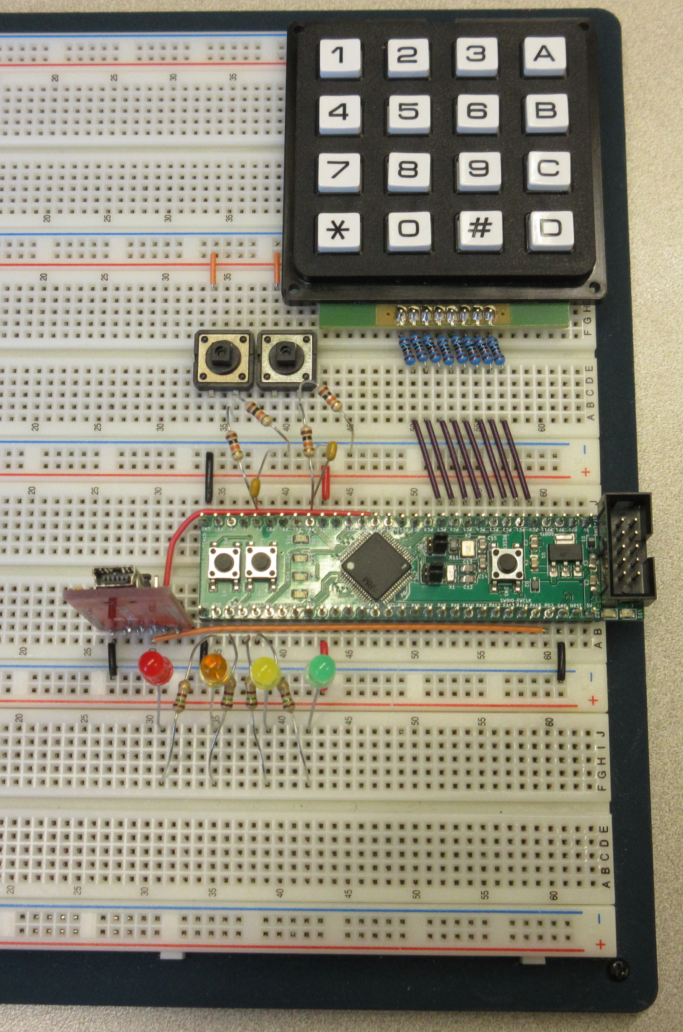
When you are finished, your circuitry should look something like below. You can, of course, arrange your circuitry in any manner you want, but we will be using the keypad in this configuration for the rest of the semester, It might be good if you keep it as close to this picture as possible. In particular, look at those blue resistors whose leads have been cut short to let them sit flush in on the breadboard. You are strongly encouraged to do the same. Later in the semester, we’ll put the resistors under the keypad, and there is no good way to do that without making the leads short. Cut each lead so that only 8mm - 10mm extends from each side. Bend the leads at an angle, and push the resistor down into the breadboard. (Resistors are inexpensive. Don’t feel bad about snipping them.)
4.6 (20 points) Buttons and LEDs
Complete the subroutine buttons in main.c. This function will be called repeatedly in a loop. The purpose of this function is to map the button presses (inputs on PB0 and PB4) to two of the 4 LEDs (on PB8-PB11). So if a button is pressed an LED should turn on and once it is released the LED should turn off. Same goes for the other button and a different LED. Pseudo-code for this function is:
void buttons(void) {
    // Use the implemented subroutines
    // Read button input at PB0
    // Put the PB0 value as output for PB8
    // Read button input at PB4
    // Put the PB4 value as output for PB9
}
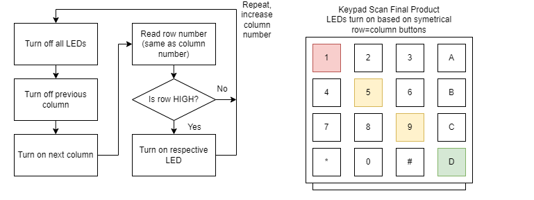
4.7 (20 points) Keypad and LEDs
Complete the subroutine keypad. It will be called in an infinte loop. The subroutine should iterate through all the column pins (PC4-PC7), setting one high and the rest low on each iteration. In each iteration, it should check all the row input values (PC0-PC3). For each column, if a button in a certain row is pressed, a light should turn on, and when it is released, it should turn off. No two columns can use buttons on the same row (the simplest arrangement will be diagonal so that only buttons on the diagonal can turn on/off the leds) and no two columns can use the same LED. Pseudo-code for this function is provided below:
void keypad(void){
    loop i = 1, 2, 3, 4 {
        set ith column to be 1 using GPIOC->ODR
        call mysleep()
        read the row inputs PC0-PC3 using GPIOC->IDR & 0xF
        check the ith row value and set this to ith LED output pin using `setn`
    }
}
Notice the function mysleep in the body of the function above. This is needed because if you were to press both the 7 and * key (for example), the light wouldn’t turn on, even though with the code above, it should. This is because the microcontroller sets and checks the pins too quickly, not giving the driving column enough time to charge the row lines (think of an RC circuit)! With the call to mysleep inserted in between the set and check, this issue is averted. mysleep can be implemented simply as an empty spinning for loop and is provided in the template:
void mysleep(void) {
    for(int n = 0; n < 1000; n++);
}
In other words, write a function to just waste some time so that we could read in the expected values.
Keypad Process Clarification
If you’d like a visualization of what’s supposed to happen, we’ve inserted a set of diagrams below. Each key turns on one LED, and their associated positions are shown on the diagram.